Solid-state image sensor and manufacturing method thereof

a solid-state image and sensor technology, applied in the direction of electrical equipment, semiconductor devices, radio frequency control devices, etc., can solve the problems of difficult to make the red (r) light pass through the aperture and reach the photoelectric conversion unit, and the difficulty of condense light which has passed through each filter film into the aperture, etc., to achieve small aperture width, small aperture width, and light-condensing efficiency

Active Publication Date: 2006-12-14
PANASONIC CORP
View PDF12 Cites 234 Cited by
  • Summary
  • Abstract
  • Description
  • Claims
  • Application Information

AI Technical Summary

Benefits of technology

[0088] Furthermore, the refractive index of the microlens in the second light-receiving cell is higher than the refractive index of the microlens in the first light-receiving cell. Accordingly, the refractive index of the microlens positioned above the light-receiving cell having a small aperture width is set to be higher than the refractive index of the microlens positioned above the light-receiving cell having a large aperture width. As a result, light-condensing efficiencies obtained by the light-receiving cell having a small aperture width and the light-receiving cell having a large aperture width can be optimized at the same time so that sensitivities of the light-receiving cells having different aperture widths can be significantly improved.
[0089] The material for the microlens or the interlayer film includes at least one of titanium oxide, tantalum oxide, niobium oxide, and hafnium oxide. Thus, the refractive index can be particularly set to be higher than the case of silicon oxide film having a refractive index of 1.45 which is commonly used as an insulating film, by using a high refractive index material such as titanium oxide, tantalum oxide, niobium oxide or hafnium oxide. Therefore, light-condensing efficiencies obtained by the light-receiving cell having a small aperture width and the light-receiving cell having a large aperture width can be optimized at the same time so that sensitivities of the light-receiving cells having different aperture widths can be significantly improved.
[0090] In the solid-state image sensor according to the present invention, the transmission wavelength band of light which passes through the aperture can be kept large even in the case where the aperture width is decreased by the use of high refractive index material having a high refractive index for the aperture in the light-blocking film formed above the photoelectric conversion unit. Accordingly, even in the case where the size of light-receiving cells in the solid-state image sensor is decreased as well as the size of the apertures, an obvious decrease in sensitivity in the longer wavelength can be prevented. Thus, a small and highly-sensitive solid-state image sensor can be realized. Furthermore, the diffusion of light above the aperture can be reduced by forming high refractive index materials in apertures so as to fill up the apertures, then forming the high refractive index materials also above the apertures, and planarizing the high refractive index materials. Thus, decrease in sensitivity is prevented while preventing the inconsistency in sensitivity among light-receiving cells so that high-quality camera can be realized. In addition, a highly-sensitive and high S/N solid-state image sensor can be realized by forming high refractive index materials in the apertures so as to fill up the apertures, then forming the high refractive index materials also above the apertures, and forming microlenses using the high refractive index materials. Consequently, a high quality-camera can be realized.
[0091] In the solid-state image sensor according to the present invention, the light condensing efficiency of light in a long wavelength is improved and the sensitivity of the photoelec...

Problems solved by technology

Furthermore, when the width of an aperture in the light-blocking film becomes smaller than the wavelength of visible light, it is difficult to condense light which has passed through each filter film into the aperture even in the case where a microlens and an intralayer len...

Method used


Image

  • Solid-state image sensor and manufacturing method thereof
  • Solid-state image sensor and manufacturing method thereof
  • Solid-state image sensor and manufacturing method thereof

Examples


second embodiment

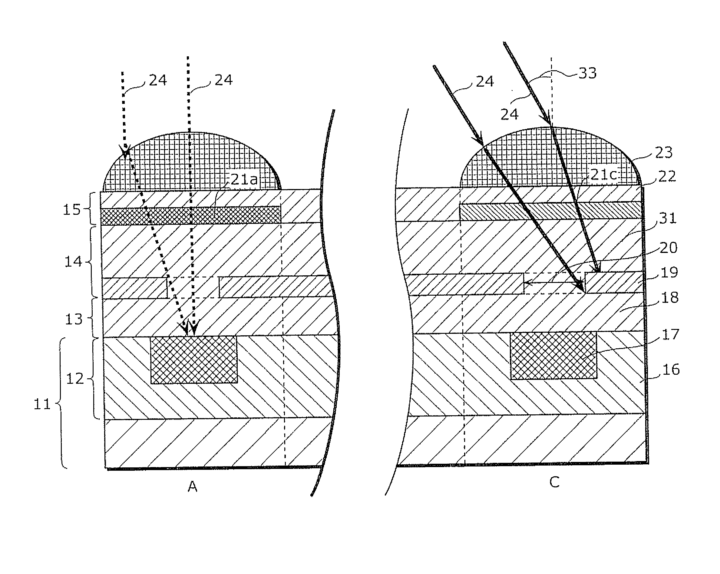
[0150]FIG. 11 is a cross-section diagram of the light-receiving cells 211a, 211b and 211c in a solid-state image sensor according to the second embodiment of the present invention. The semiconductor substrate 11, the photoelectric conversion layer 12 and the insulating layer 13 of each light-receiving cell has the same configuration as in the conventional light-receiving cell shown in FIG. 3.

[0151] While a metal layer 214 includes a light-blocking film 19 as in the case of the conventional solid-state image sensor, in the solid-state image sensor according to the second embodiment of the present invention, the metal layer 214 has a high refractive index layer 225 that is formed by applying a high refractive index material in and on an aperture 20 in the light-blocking film 19 after the formation of the light-blocking film 19. Herein, the high-refractive index layer 225 is processed into a shape of a convex intralayer lens. Accordingly, the interlayer film 29 and the intralayer lens...

third embodiment

[0161]FIG. 13 is a cross-section diagram of the light-receiving cells 311a, 311b and 311c in a solid-state image sensor according to the third embodiment of the present invention.

[0162] The solid-state image sensor of the third embodiment is is different from the solid-state image sensor of the first embodiment in that the insulating layer 13, the metal layer 114 and the microlens 23 have the same refractive index value.

[0163] In the solid-state image sensor of the third embodiment, a light-receiving cell having a longer transmission wavelength of a filter has higher refractive indexes of the insulating film 13, an insulating layer in the metal layer 114 and a microlens 23. In addition, light receiving cells having different transmission wavelengths of respective filters have different refractive indexes of the insulating layer 13, insulating layer in the metal layer 114, and microlens 23. For example, in the light-receiving cell having a longer transmission wavelength of a filter...

fourth embodiment

[0164]FIG. 14 is a cross-section diagram of the light-receiving cells 411a, 411b and 411c in a solid-state image sensor according to the fourth embodiment of the present invention. The semiconductor substrate 11, photoelectric conversion layer 12, insulating layer 13, and metal layer 14 and color filter 15 of each light-receiving cell in the fourth embodiment has the same configuration as in the conventional solid-state image sensor shown in FIG. 3 except that the intralayer lens 30 is not formed in the metal layer 14 in the present embodiment.

[0165] The solid-state image sensor of the fourth embodiment has a configuration in which a refractive index of a material which composes the microlens 423 formed on the color filter layer 15 differs in accordance with a transmission wavelength band of a color filter.

[0166] Here, the finer the light-receiving cells are, the narrower the widths of the apertures 20 become. For example, when the width of the aperture 20 is 2 μm or smaller, it i...


PUM


Abstract

An object of the present invention is to provide a small solid-state image sensor which realizes significant improvement in sensitivity. The solid-state image sensor of the present invention includes a semiconductor substrate in which photoelectric conversion units are formed, a light-blocking film which is formed above the semiconductor substrate and has apertures formed so as to be positioned above respective photoelectric conversion units, and a high refractive index layer formed in the apertures. Here, each aperture has a smaller aperture width than a maximum wavelength in a wavelength of light in a vacuum converted from a wavelength of the light entering the photoelectric conversion unit through the apertures, and the high refractive index is made of a high refractive index material having a refractive index which allows transmission of light having the maximum wavelength through the aperture.

Description

BACKGROUND OF THE INVENTION [0001] (1) Field of the Invention [0002] The present invention relates to a solid-state image sensor used for a digital camera and the like, and particularly to light-receiving cells which constitute the solid-state image sensor. [0003] (2) Description of the Related Art [0004] A general solid-state image sensor includes plural light-receiving cells formed on a semiconductor substrate, each of which has a photoelectric conversion unit which converts incident light entering through an aperture in a light-blocking film into signal charge and a color filter which is formed on the light-blocking film and separates the incident light based on colors. A primary color filter or a complementary color filter is commonly used as a color filter. Red (R), blue (B) and green (G) are used for primary color filters, and cyan (C), magenta (M) and yellow (Y) that are complementary colors of red, green and blue are respectively used for complementary color filters. In gene...

Claims


Application Information

Patent Timeline
IPC IPC(8): H01L31/00
CPCH01L27/1462H01L27/14621H01L27/14623H01L27/14687H01L27/14627H01L27/14632H01L27/14685H01L27/14625
Inventor YAMAGUCHI, TAKUMIMURATA, TAKAHIKOKASUGA, SHIGETAKA
Owner PANASONIC CORP
Why Eureka
Try Eureka