Image formation device and image formation process
a technology of image formation device and image, which is applied in the direction of electrostatic process equipment, instruments, developers, etc., can solve the problems of large latent image charge amount of carlson method, small contrast, and inability to recover electrostatically toner at the exposure portion
- Summary
- Abstract
- Description
- Claims
- Application Information
AI Technical Summary
Problems solved by technology
Method used
Image


Examples
first embodiment
[0046] As shown in FIG. 6, a color laser printer (hereafter referred to simply as a printer) which serves as an image formation device of a first embodiment is structured with printing sections 12Y, 12M, 12C and 12K (hereafter referred to as “printing sections 12Y to 12K”) arranged in this order from upstream to downstream along a conveyance direction (the direction of arrow T). The printing sections 12Y to 12K transfer respective toner images of the colors yellow (Y), magenta (M), cyan (C) and black (K) to continuous paper P, which serves as an object of transfer, superposing the toner images of the respective colors to form an image.
[0047] At a conveyance direction upstream side of the printing sections 12Y to 12K, a paper conveyance section (which is not illustrated) is provided. Meanwhile, a fixing section (not shown) and an ejection section (not shown) are provided at a conveyance direction downstream side of the printing sections 12Y to 12K. The fixing section fixes unfixed t...
second embodiment
[0083] Now, a second embodiment of the present invention will be described. For this second embodiment, structural portions that are the same as in the first embodiment are assigned the same reference numerals, and descriptions of these structures will be omitted.
[0084] Features of the second embodiment are that a power source for separation discharge prevention is provided, separately from the power source which applies the latent image formation voltage, and applies a voltage for separation discharge prevention, and that the separation discharge prevention voltage is applied in the second step in addition to the application of the latent image formation voltage.
[0085] First, a principle of operation of the second embodiment will be described.
[0086] As shown in FIG. 9A, when the latent image formation voltage is applied to the charge conservation member via the voltage supply section, which is a conductive layer, positive charge is induced in the transparent conductive substrate...
example 1-1
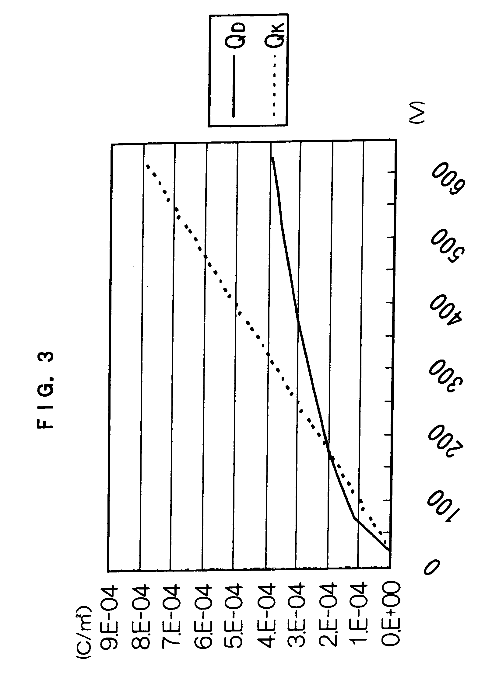
[0101] First, an Example 1-1 of the first embodiment will be described. The photoconductive drum 20 of Example 1-1 is prepared by: applying 4 μm of a one-layer organic photoconductive layer by a coating method, to serve as the photoconductive layer; thereon, by a mask deposition method, sputtering copper in a pattern finer than a pixel density to structure a layer, of dots with a spacing of 2 μm and an isolated dot electrode diameter of 1 μm, to a thickness of 0.5 μm; and thereon, coating an insulative resin to 1 μm. Diameter of the photoconductive drum 20 is 240 mm. A process speed of Example 1-1, that is, a paper conveyance speed, is 1.0 m / s.
[0102] The conductive rubber roller 42 is structured by covering a core fixture which serves as a roller shaft with a resilient member. The resilient member has a single layer structure in which conductive carbon is dispersed, and a resistance value thereof is 108 to 109Ω. A roller diameter is a diameter of 30 mm (with a conventional corona c...
PUM
 Abstract
Description
Claims
Application Information
 - R&D
- Intellectual Property
- Life Sciences
- Materials
- Tech Scout
- Unparalleled Data Quality
- Higher Quality Content
- 60% Fewer Hallucinations
Browse by: Latest US Patents, China's latest patents, Technical Efficacy Thesaurus, Application Domain, Technology Topic, Popular Technical Reports.
© 2025 PatSnap. All rights reserved.Legal|Privacy policy|Modern Slavery Act Transparency Statement|Sitemap|About US| Contact US: help@patsnap.com