
Single plate-type color solid-state image sensing device

a color solid-state image and sensing device technology, applied in the direction of radio frequency controlled devices, television system scanning details, television systems, etc., can solve the problems of large number of levels or defects, and large time (referred to as “dark current”), so as to reduce the effect of dark curren

Active Publication Date: 2006-09-28
FUJIFILM CORP +1
View PDF17 Cites 22 Cited by
  • Summary
  • Abstract
  • Description
  • Claims
  • Application Information

AI Technical Summary

Benefits of technology

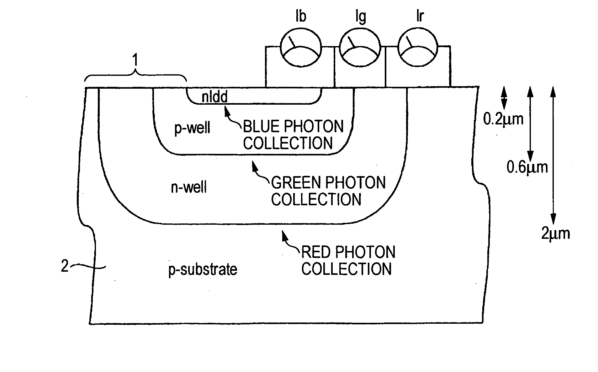
The invention provides a single plate-type color solid-state image sensing device that can reduce dark current and improve image quality. The device includes a semiconductor substrate with signal reading circuits and high density impurity regions, a blue light detecting photodiode, a red light detecting photodiode, and a green light detecting photodiode. The device also includes MOS switches for transferring electric charge accumulated in a charge storage layer of each photodiode to corresponding one of the high density impurity regions. By forming connection regions only in portions adjacent to the high density impurity regions, the device can reduce dark current and improve image quality.

Problems solved by technology

In the hybrid-type image sensing device described in JP-A-2003-332551, like the image sensing device described in JP-A-2002-513145, there is however a problem that an output at dark time (referred to as “dark current”) is so large that the image quality of a dark portion of a subject is particularly poor.
A very large number of levels or defects which will serve as sources for generating dark current are present in the interfaces.
The dark current (or output at dark time) severs as fixed-pattern noise or random noise, so that image quality is deteriorated remarkably.

Method used


Image

  • Single plate-type color solid-state image sensing device
  • Single plate-type color solid-state image sensing device
  • Single plate-type color solid-state image sensing device

Examples


first embodiment

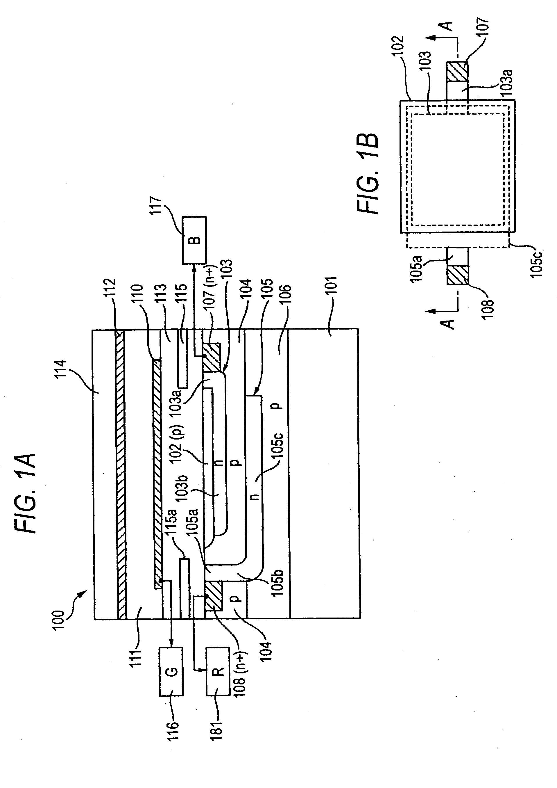
[0031]FIG. 1A is a schematic sectional view of one of unit cells in a single plate-type color solid-state image sensing device according to a first embodiment of the invention. FIG. 1B is a schematic plan view of a surface portion of a silicon substrate in the single plate-type color solid-state image sensing device depicted in FIG. 1A. A section taken along the line A-A in FIG. 1B is shown in FIG. 1A. Unit cells as shown in FIG. 1A are arranged two-dimensionally lengthwise and widthwise to form an image sensing device.

[0032] A single plate-type color solid-state image sensing device 100 according to this embodiment is of a hybrid type. In the single plate-type color solid-state image sensing device 100, two photodiodes are formed in an n-type silicon substrate 101 so that the quantity of incident blue (B) light and the quantity of incident red (R) light can be detected by the photodiodes respectively. A photoelectric conversion film 111 is laminated as an upper layer on the silico...

second embodiment

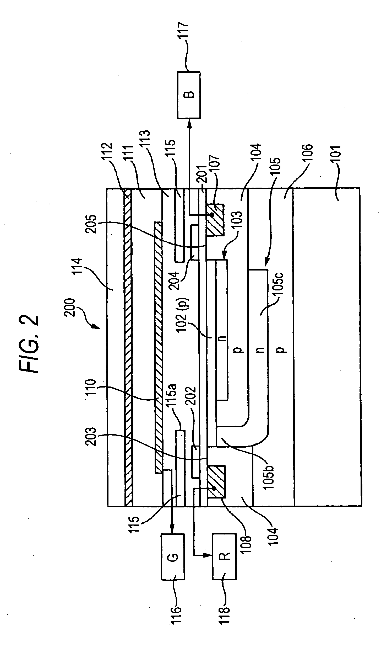
[0058]FIG. 2 is a schematic sectional view of one of unit cells in a single plate-type color solid-state image sensing device according to a second embodiment of the invention. Constituent parts identical or equivalent to those of the single plate-type color solid-state image sensing device according to the first embodiment are referred to by the same numerals correspondingly, and description only about different parts will be made below.

[0059] A single plate-type color solid-state image sensing device 200 according to this embodiment has a gate electrically insulating film 201 formed on an outermost surface of a silicon substrate 101, and a transparent electrically insulating film 113 laminated on the gate electrically insulating film 201.

[0060] A charge passage portion 105b is formed in an n-type semiconductor layer 105 so that an upper end portion of the charge passage portion 105b is stopped in position abutting on a p-type semiconductor layer 102. That is, the n-type semicond...

third embodiment

[0065]FIG. 3 is a schematic sectional view of a single plate-type color solid-state image sensing device according to a third embodiment of the invention. In a single plate-type color solid-state image sensing device 300 according to this embodiment, three photodiode structures are provided in an n-type silicon substrate 301 so that the three colors of R, G and B are separated and detected. That is, a p-type semiconductor layer 308, an n-type semiconductor layer 307, a p-type semiconductor layer 306, an n-type semiconductor layer 305, a p-type semiconductor layer 304, an n-type semiconductor layer 303 and a p-type semiconductor layer 302 are provided in order viewed from a deep portion of the silicon substrate 301. A transparent electrically insulating film 312 is laminated on the surface of the silicon substrate 301. In addition, a shading film 313 provided with openings 313a is buried in the transparent electrically insulating film 312.

[0066] N-type high density impurity regions ...


PUM


Abstract

A color solid-state image sensing device including: a semiconductor substrate having a surface portion where high density impurity regions connected to signal reading circuits respectively are formed; a blue light detecting photodiode formed in a shallow portion of the semiconductor substrate; and a red light detecting photodiode formed in a deep portion of the semiconductor substrate, wherein connection regions which are provided so as to be continued to the photodiodes respectively and exposed to the surface of the semiconductor substrate are formed only in portions adjacent to the high density impurity regions so that electric charge accumulated in each photodiode can be transferred to corresponding one of the corresponding high density impurity regions.

Description

FIELD OF THE INVENTION [0001] The present invention relates to a single plate-type color solid-state image sensing device for detecting signals of the three colors of red (R), green (G) and blue (B) per pixel. Particularly, it relates to a single plate-type color solid-state image sensing device which can sense a high-quality color image while dark current is reduced. BACKGROUND OF THE INVENTION [0002] In a background-art single plate-type color solid-state image sensing device represented by a CCD image sensor or a CMOS image sensor, respective color filters of R, G and B are mounted mosaically on an array of photoelectric conversion pixels (photodiodes). Color signals outputted from the respective pixels of the color solid-state image sensing device in accordance with the color filters are processed to generate a color image. [0003] In the color solid-state image sensing device having the color filters arranged mosaically, when color filters of the three primary colors (R, G and B...

Claims


Application Information

Patent Timeline
Patent Type & Authority Applications(United States)
IPC IPC(8): H04N9/04H01L27/146H01L31/10H01L51/42H04N23/12H04N25/00
CPCH01L27/14647H04N25/76H04N25/17
Inventor SUZUKI, NOBUO
Owner FUJIFILM CORP
Learn More