Photovoltaic device
a photovoltaic device and photovoltaic technology, applied in the field of photovoltaic devices, can solve the problems of increasing the open-circuit voltage of the photovoltaic device, and achieve the effects of increasing the built-in electric field, increasing the open-circuit voltage of the photovoltaic device, and increasing the band gap
- Summary
- Abstract
- Description
- Claims
- Application Information
AI Technical Summary
Benefits of technology
Problems solved by technology
Method used
Image

Examples
embodiment 1
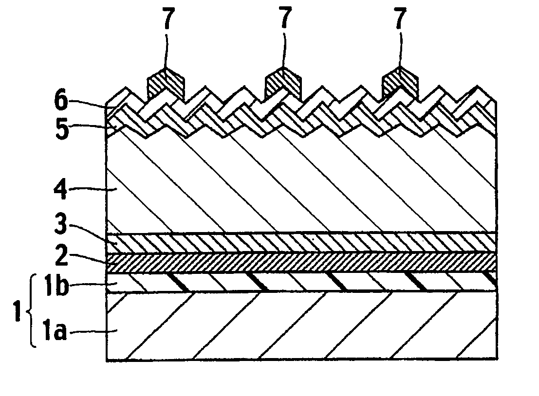
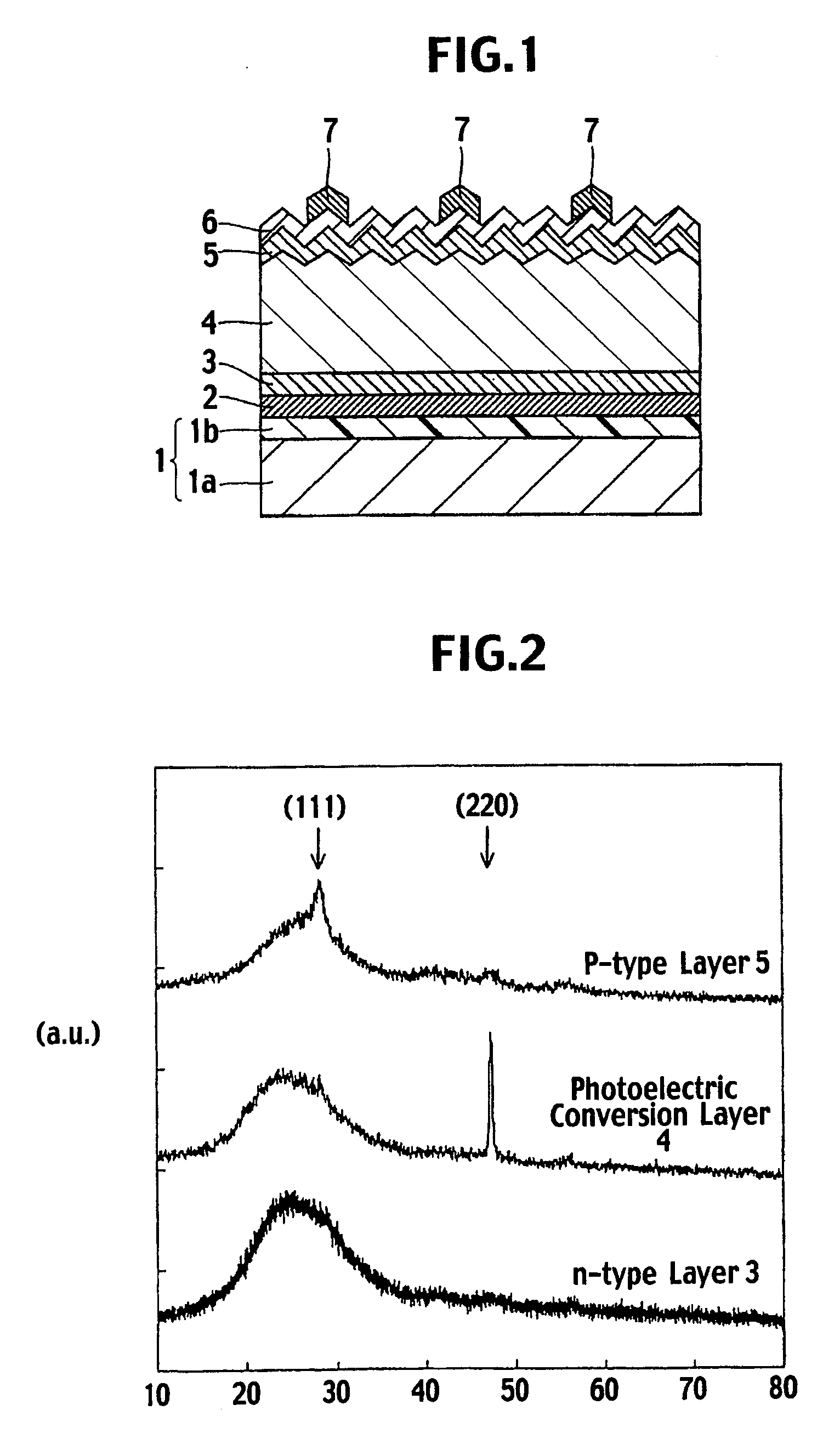
[0037]FIG. 1 is a sectional view showing the structure of a photovoltaic device according to an embodiment 1 of the present invention. The structure of the photovoltaic device according to the embodiment 1 will be explained with reference to FIG. 1.
[0038] The photovoltaic device according to the embodiment 1 has a stainless plate (SUS430) 1a that is 0.15 mm thick and is flat. Formed on the stainless plate 1a is a polyimide resin layer 1b of 20 μm thick. The stainless plate 1a and polyimide resin layer 1b form a substrate 1 having a flat surface. Formed on the substrate 1 (polyimide resin layer 1b) is a rear electrode 2 that is 200 nmthick, is made of Ag (silver), and is flat.
[0039] Sequentially formed on the rear electrode 2 are an n-type layer 3, a photoelectric conversion layer 4, and a p-type layer 5 having thicknesses of 20 nm, 2 μm, and 20 nm, respectively. The n-type layer 3, photoelectric conversion layer 4, and p-type layer 5 form a power generation unit.
[0040] According ...
embodiment 2
[0080]FIG. 9 is a sectional view showing the structure of a photovoltaic device according to an embodiment 2 of the present invention. Unlike the embodiment 1, the embodiment 2 employs an n-type layer having a preferred orientation plane of (111), a photoelectric conversion layer having a preferred orientation plane of (220), and an amorphous p-type layer. The structure of the photovoltaic device according to the embodiment 2 will be explained with reference to FIG. 9.
[0081] Like the embodiment 1, the photovoltaic device of the embodiment 2 shown in FIG. 9 employs a stainless plate 1a and a polyimide resin layer 1b to form a substrate 1. On the substrate 1, a rear electrode 2 is formed. On the rear electrode 2, the n-type layer 43, photoelectric conversion layer 44, and p-type layer 45 are sequentially formed to have thicknesses of 50 nm, 2 μm, and 15 nm, respectively. The n-type layer 43, photoelectric conversion layer 44, and p-type layer 45 form a power generation unit.
[0082] A...
embodiment 3
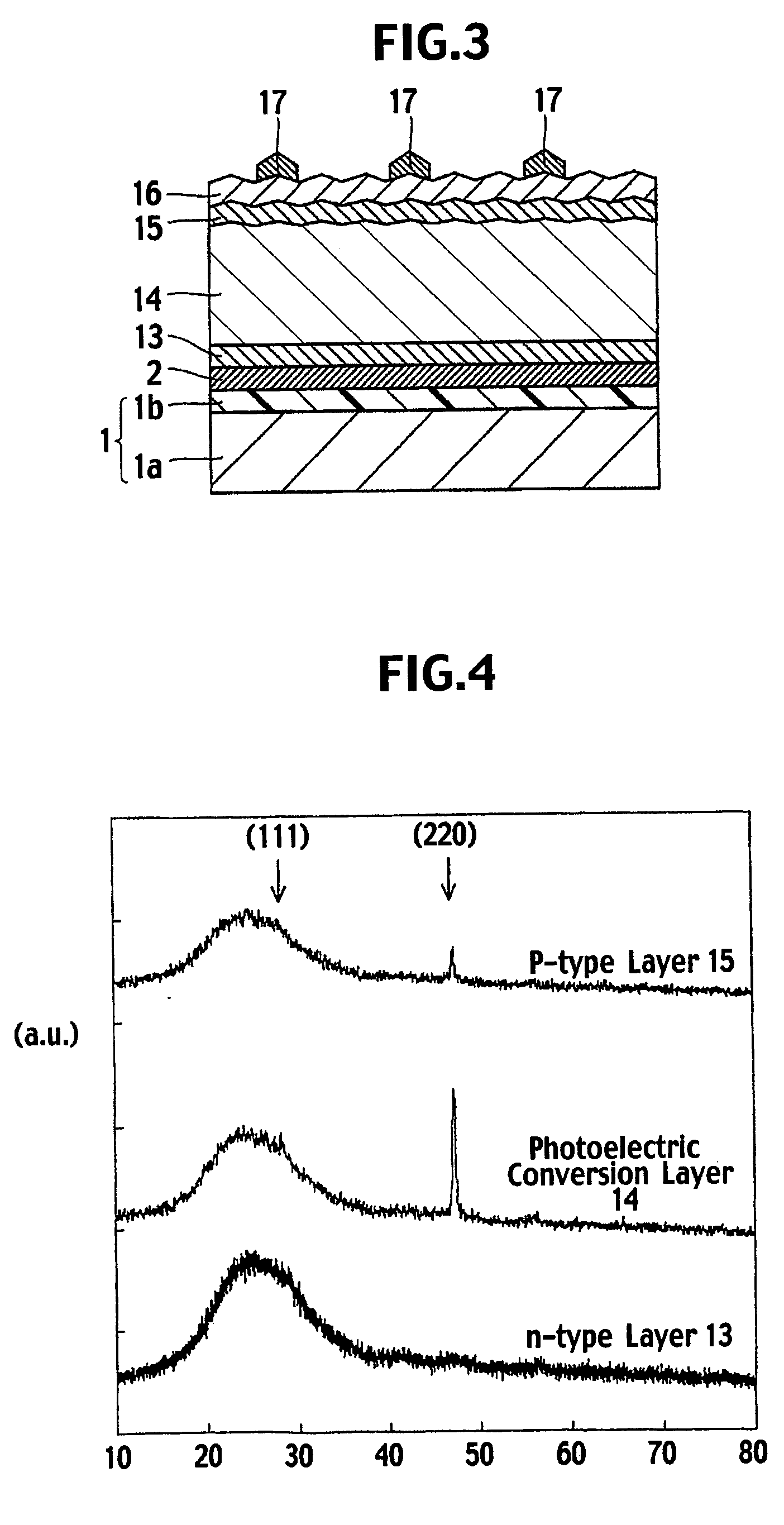
[0113]FIG. 15 is a sectional view showing the structure of a photovoltaic device according to an embodiment 3 of the present invention. Unlike the embodiments 1 and 2, the embodiment 3 employs a p-type layer having a two-layer structure. The structure of the photovoltaic device according to the embodiment 3 will be explained.
[0114] Like the embodiment 1, the photovoltaic device of the embodiment 3 shown in FIG. 15 employs a stainless plate 1a and a polyimide resin layer 1b to form a substrate 1. On the substrate 1, a rear electrode 2 is formed. On the rear electrode 2, an n-type layer 73, a photoelectric conversion layer 74, and the p-type layer 75 are sequentially formed to have thicknesses of 50 nm, 2 μm, and 20 nm, respectively. The p-type layer 75 includes a first p-type layer 75a formed on the photoelectric conversion layer 74 to a thickness of 15 nm and a second p-type layer 75b formed on the first p-type layer 75a to a thickness of 5 nm. The n-type layer 73, photoelectric co...
PUM
 Abstract
Description
Claims
Application Information
 - R&D
- Intellectual Property
- Life Sciences
- Materials
- Tech Scout
- Unparalleled Data Quality
- Higher Quality Content
- 60% Fewer Hallucinations
Browse by: Latest US Patents, China's latest patents, Technical Efficacy Thesaurus, Application Domain, Technology Topic, Popular Technical Reports.
© 2025 PatSnap. All rights reserved.Legal|Privacy policy|Modern Slavery Act Transparency Statement|Sitemap|About US| Contact US: help@patsnap.com