Eureka AIR delivers breakthrough ideas for toughest innovation challenges, trusted by R&D personnel around the world.

Semiconductor light emitting devices and methods

a technology of semiconductors and light emitting devices, applied in semiconductor devices, lasers, semiconductor lasers, etc., can solve the problems of fundamental limitations of bipolar transistor speed, spontaneous emission recombination lifetime, etc., to promote carrier transport unidirectionally, light emission and device speed are both enhanced, and the directionality and speed of carrier transport is improved

Inactive Publication Date: 2006-09-21
THE BOARD OF TRUSTEES OF THE UNIV OF ILLINOIS
View PDF11 Cites 23 Cited by
  • Summary
  • Abstract
  • Description
  • Claims
  • Application Information

AI Technical Summary

Benefits of technology

"The patent text describes a method for producing an optical output from a bipolar light-emitting transistor device. The method involves modulating the base current to produce light emission, and utilizing stimulated emission to enhance the speed of the transistor. The use of quantum size effects in the base layer of the transistor can also enhance the speed of the device. The patent also describes a semiconductor laser that includes a heterojunction bipolar transistor structure and an optical resonant cavity. The method can be used in high-speed bipolar transistors and light emitting bipolar transistors. The patent also describes a device and technique for generating optical signals with an enhanced signal to noise ratio and control of on and off time durations."

Problems solved by technology

Spontaneous emission recombination lifetime is a fundamental limitation of bipolar transistor speed.

Method used


Image

  • Semiconductor light emitting devices and methods
  • Semiconductor light emitting devices and methods
  • Semiconductor light emitting devices and methods

Examples


Embodiment Construction

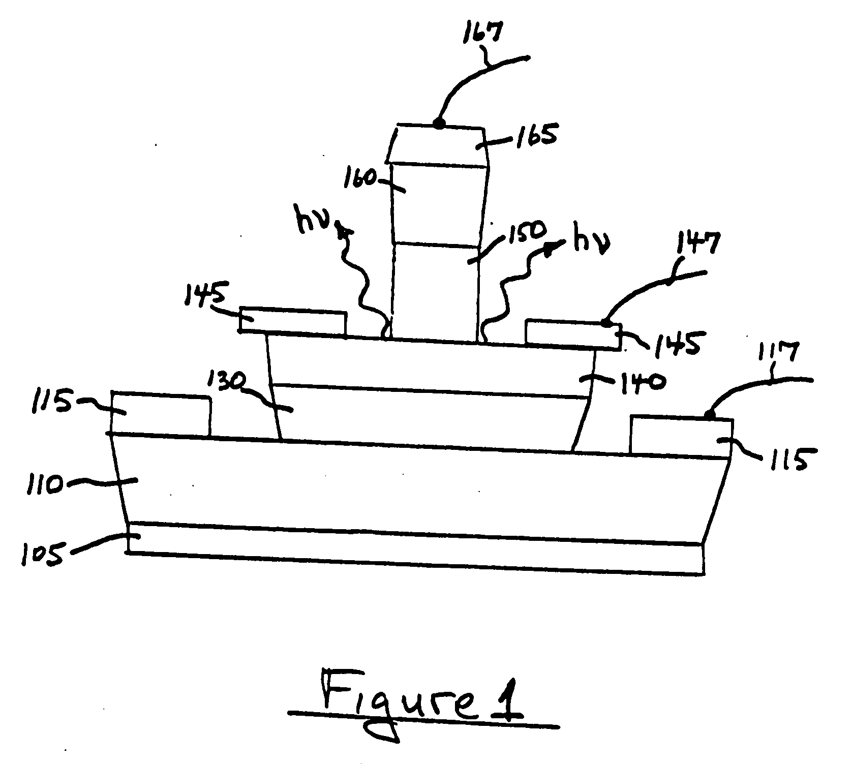
[0029]FIG. 1 illustrates a device as described in the referenced prior applications. A substrate 105 is provided, and the following layers are disposed thereon: subcollector 110, collector 130, base 140, emitter 150, and cap layer 160. Also shown are collector metallization (or electrode) 115, base metallization 145, and emitter metallization 165. Collector lead 117, base lead 147, and emitter lead 167 are also shown. In a described form of this device, the layers were grown by MOCVD, and the collector layer 130 comprised 3000 Angstrom thick n-type GaAs, n=2×1016 cm−3, the base layer 140 comprised 600 Angstrom thick p+ carbon-doped compositionally graded InGaAs (1.4% In), p=4.5×1019 cm−3, the emitter layer 150 comprised 800 Angstrom thick n-type InGaP, n=5×1017 cm−3, and the cap layer comprised 1000 Angstrom thick n+ InGaAs, n=3×1019 cm−3.

[0030] The fabrication process sequence included e-beam defined Ti / Pt / Au emitter contacts (165), a self-aligned emitter etch, a self-aligned Ti / P...


PUM


Abstract

A method for producing an optical output, including the following steps: providing first and second electrical signals; providing a bipolar light-emitting transistor device that includes collector, base, and emitter regions; providing a collector electrode coupled with the collector region and an emitter electrode coupled with the emitter region, and coupling electrical potentials with respect to the collector and emitter electrodes; providing an optical coupling in optical communication with the base region; providing first and second base electrodes coupled with the base region; and coupling the first and second electrical signals with the first and second base electrodes, respectively, to produce an optical output emitted from the base region and coupled into the optical coupling, the optical output being a function of the first and second electrical signals.

Description

PRIORITY CLAIMS [0001] The present application is a continuation-in-part of U.S. patent application Ser. No. 11 / 068,561, filed Feb. 28, 2005, which is, in turn, a continuation-in-part of two U.S. patent applications (Ser. No. 10 / 861,103, filed Jun. 4, 2004, and Ser. No. 10 / 861,320, filed Jun. 4, 2004) each of these two last-mentioned Applications being, in turn, a continuation-in-part of U.S. patent application Ser. No. 10 / 646,457, filed Aug. 22, 2003. GOVERNMENT RIGHTS [0002] This invention was made with Government support under Contract Number HR 0011-04-1-0034 awarded by the Defense Advanced Research Projects Agency (DARPA). The Government has certain rights in the invention.FIELD OF THE INVENTION [0003] This invention relates to semiconductor light emitting devices and methods, and also to devices and methods that include wave mixing modulation laser transistors and techniques. BACKGROUND OF THE INVENTION [0004] A part of the background hereof lies in the development of light em...

Claims


Application Information

Patent Timeline
Patent Type & Authority Applications(United States)
IPC IPC(8): H01L31/113
CPCB82Y20/00H01S5/06203H01S5/06226H01S5/18341H01S5/305H01S5/3095H01S5/3211H01S5/3412H01S5/34313H01S5/4031H01S3/10
Inventor FENG, MILTONHOLONYAK, NICK JR.CHAN, RICHARD
Owner THE BOARD OF TRUSTEES OF THE UNIV OF ILLINOIS
Why Eureka
Eureka Blog
Learn More