MEMS device package and method of manufacturing the same

a technology of micro electromechanical system and device package, which is applied in the direction of semiconductor devices, instruments, electrical apparatus, etc., can solve the problems of reducing yield and productivity, requiring a lot of time, and affecting the miniaturization of appliances, so as to achieve the effect of simplifying the manufacturing process and miniaturizing the size of the mems device packag

Inactive Publication Date: 2006-09-07
SAMSUNG DISPLAY CO LTD
View PDF4 Cites 17 Cited by
  • Summary
  • Abstract
  • Description
  • Claims
  • Application Information

AI Technical Summary

Benefits of technology

[0014] According to one aspect, the present invention provides a MEMS device package which employs a cap substrate formed from the same material as a device substrate, so that stress caused due to the difference in thermal expansion coefficient between the cap substrate and the device substrate, the manufacturing process of the MEMS device package can be simplified, and the size of the MEMS device package can be miniaturized, and a method of manufacturing such a MEMS device package.

Problems solved by technology

Consequently, the above-mentioned conventional package contributes to an obstruction in miniaturizing an appliance which employs such a MEMS package, because it is high and large in size and thus occupies a large volume in the appliance.
Furthermore, by employing the glass-based covering substrate 3, the above-mentioned conventional MEMS device package has a problem in that the processes for forming the via holes 6 for electrode-wiring and the outer electrode pads 7 are very complicated and require a lot of time, thereby causing a drop in yield and productivity.
The conventional MEMS package also has a problem in that the MEMS active device 2 may be deformed or damaged due to high temperature at the time of anodic-bonding (typically, about 460° C.) and inherent stress is included due to the difference in thermal expansion coefficient between the covering glass substrate 3 and the device substrate 1.
In addition, the circuit connection between the inner electrode pads 4 formed from silicon and the outer electrode pads 7 formed from a metallic material such as aluminum (Al) may present a problem in terms of reliability of the device because such a circuit connection generates very high inductance in connection with the electric contact resistance at the contact areas and RF of high frequency, thereby causing a great signal loss.
Meanwhile, existing bonding materials such as SnPb are spread out laterally when bonding a wafer and a glass material, whereby uniformity may be deteriorated or poor quality may be frequently caused in forming a rim of the package.

Method used


Image

  • MEMS device package and method of manufacturing the same
  • MEMS device package and method of manufacturing the same
  • MEMS device package and method of manufacturing the same

Examples


Embodiment Construction

[0035] Hereinbelow, a MEMS device package according to an exemplary embodiment of the present invention is described in detail with reference to accompanying drawings. The described exemplary embodiments are intended to assist the understanding of the invention and are not intended to limit the scope of the invention in any way.

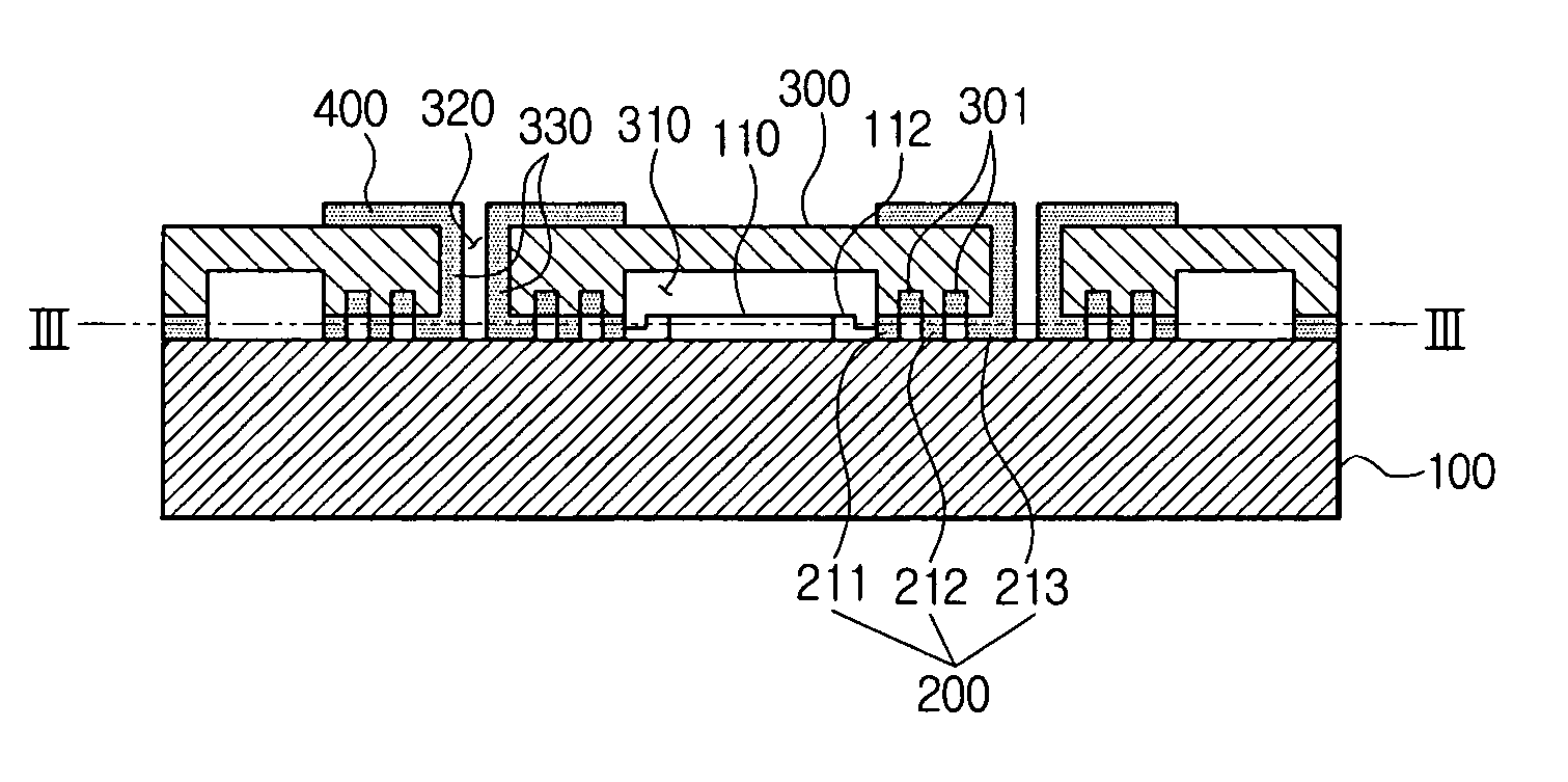
[0036]FIG. 2 is a schematic cross-sectional view showing a structure of a MEMS device package according to an exemplary embodiment of the present invention. As shown in the drawing, the MEMS device package includes a device substrate 100, multiple sealing pads 200, a cap substrate 300, and outer electrode pads 400. The device substrate 100 and the cap substrate 300 are formed from silicon wafers of an identical material.

[0037] A MEMS active device 110 is formed at the center of the top surface of the device substrate 100. Typically, the MEMS active device 110 comprises an elastic member, a stage supported by the elastic member, and electric electrodes for s...


PUM


Abstract

A MEMS device package and a method of manufacturing the same. The MEMS device package includes a device substrate having a surface on which a MEMS active device is formed, and multiple sealing pads arranged around the MEMS active device so that the sealing pads provide electric paths for the MEMS active device. In addition, the MEMS device package may include a cap substrate bonded to the device substrate through the multiple sealing pads, the cap substrate including a trench, within which the MEMS active device is positioned, and via holes. One or more outer electrode pads may be formed on one surface of the cap substrate to be electrically connected with the multiple sealing pads through the via holes. Because there are several bonding and sealing areas between the device substrate and the cap substrate, the sealing intensity is strengthened.

Description

CROSS-REFERENCE TO RELATED APPLICATIONS [0001] This application claims priority from Korean Patent Application No. 2005-18682, filed Mar. 7, 2005, in the Korean Intellectual Property Office, the entire disclosure of which is incorporated herein by reference. BACKGROUND OF THE INVENTION [0002] 1. Field of the Invention [0003] The present invention relates to a MEMS (Micro Electro-Mechanical System) device package and a method of manufacturing the same. [0004] 2. Description of the Related Art [0005] The field of MEMS is a technical field for processing sensors, micro-actuators, gyroscopes, or parts for precise machines using a semiconductor processing technique. Therefore, the use of MEMS is considered as a technique for improving performance and reducing costs as the precise workability, uniformity between products, superior productivity, etc., of the semiconductor technique can be applied to MEMS. [0006] MEMS devices, for example, accelerometers, angular velocity sensors, resonance...

Claims


Application Information

Patent Timeline
Patent Type & Authority Applications(United States)
IPC IPC(8): H01L21/00
CPCB81B7/0051B81B7/007H01L2924/16235B81B7/02
Inventor KIM, JONG-SEOKKIM, DUCK-HWANNAM, KUANG-WOOPARK, YUN-KWONYUN, SEOK-CHULCHOA, SUNG-HOONSONG, IN-SANG
Owner SAMSUNG DISPLAY CO LTD
Why Eureka
Try Eureka