Adjustment of termination resistance in an on-die termination circuit

a termination circuit and resistance technology, applied in the field of on-die termination circuits, can solve the problems of nonlinear change of resistance, circuit suffers, impedance varies widely according to the situation, etc., and achieve the effect of suppressing the fluctuation of termination resistan

Active Publication Date: 2006-09-07
LONGITUDE LICENSING LTD
View PDF7 Cites 2 Cited by
  • Summary
  • Abstract
  • Description
  • Claims
  • Application Information

AI Technical Summary

Benefits of technology

[0047] It is an object of the present invention to provide an on-die termination circuit that, during adjustment of termination resistance, can keep the termination resistance close to the target value even within the high-frequency region, and moreover, that can suppress the fluctuation of termination resistance that results from differences in the configuration of parasitic elements.
[0051] According to this configuration, the amount of fluctuation of the resistance of the resistance elements of the main resistance circuit during adjustment of the termination resistance is adjusted by turning the transistors of the adjustment circuit ON and OFF. In other words, the transistors of the adjustment circuit are components provided for adjusting the amount of fluctuation of the resistance of resistance elements, and because the transistors of the adjustment circuit are connected in parallel with the main resistance circuit, are able to set the resistance to a higher level.
[0053] As a result, the frequency dependency of the on-die termination circuit overall can be reduced, and the fluctuation of the termination resistance depending on frequency can be suppressed. The termination resistance can therefore be maintained at a value relatively close to the target value even in the high-frequency region.
[0054] In addition, the impedance of transistors that are OFF can be ignored despite variations in transistors that are ON when adjusting the termination resistance and the consequent changes in the parasitic element configuration of these parts. The termination resistance of the entire on-die termination circuit can therefore be kept substantially uniform, whereby fluctuations in the termination resistance that result from variation in the configuration of parasitic elements can also be suppressed even in the high-frequency region.

Problems solved by technology

However, because the on-die termination circuit of the first example of the prior art shown in FIG. 1 is composed solely of transistors p1˜p5 which are PMOS transistors, the circuit suffers from the problem that the impedance varies widely according to the voltage level of Vswing due to the characteristics of MOS transistors.
However, in the linear region in which VDS increases and approaches the saturation region, the change in resistance becomes nonlinear and can no longer be treated as normal linear resistance.
Consequently, the reflection of the bus signals transferred through the transfer bus has an adverse effect on signal transmission.
If operation at low voltage is desired for the sake of reducing power consumption, however, transistors p1˜p5 will operate in the-saturation region as described above when the power supply voltage reaches the level of 1.8V, and the termination resistance can no longer be maintained at a fixed level.
As previously explained, the termination resistance is highly dependent on frequency when adjusting the termination resistance in an on-die termination circuit of the prior art and the prior art therefore suffers from the problem that the termination resistance is lower than the target value in the high-frequency region.
A difference in the transistors that are ON when adjusting the termination resistance raises the problem that the parasitic element configuration of these parts also differs, whereby the frequency characteristic changes and the termination resistance at which stability is attained in the high-frequency region varies greatly.

Method used


Image

  • Adjustment of termination resistance in an on-die termination circuit
  • Adjustment of termination resistance in an on-die termination circuit
  • Adjustment of termination resistance in an on-die termination circuit

Examples


first embodiment

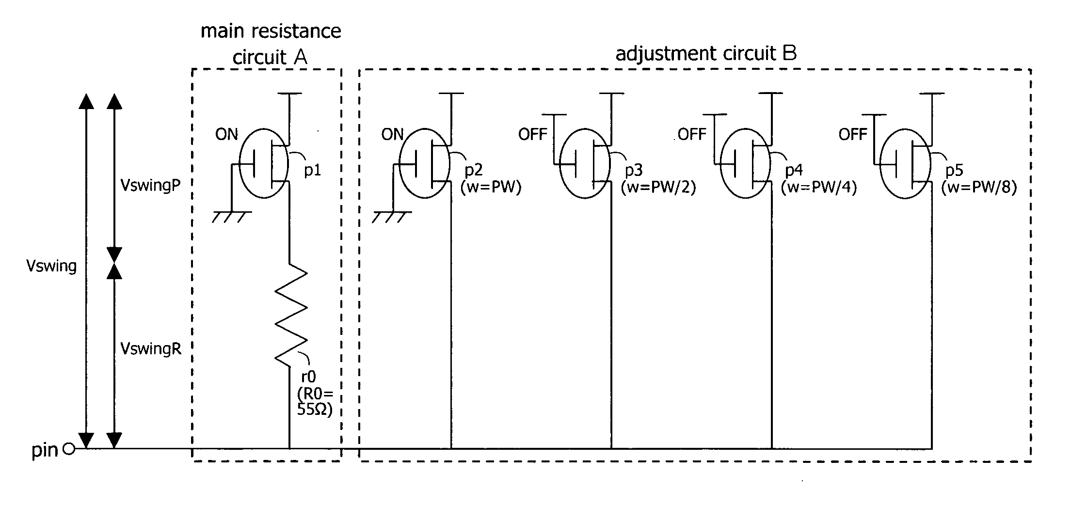
[0078]FIGS. 10A and 11A show the configuration of the on-die termination circuit of the first embodiment of the present invention. Although the circuit configuration itself is identical in FIGS. 10A and 11A, the transistors that are ON during the adjustment of termination resistance are different. FIG. 10B shows an equivalent circuit diagram in which FIG. 10A is represented by resistance elements and capacitance elements, and FIG. 11B shows an equivalent circuit diagram in which FIG. 11A is represented by resistance elements and capacitance elements.

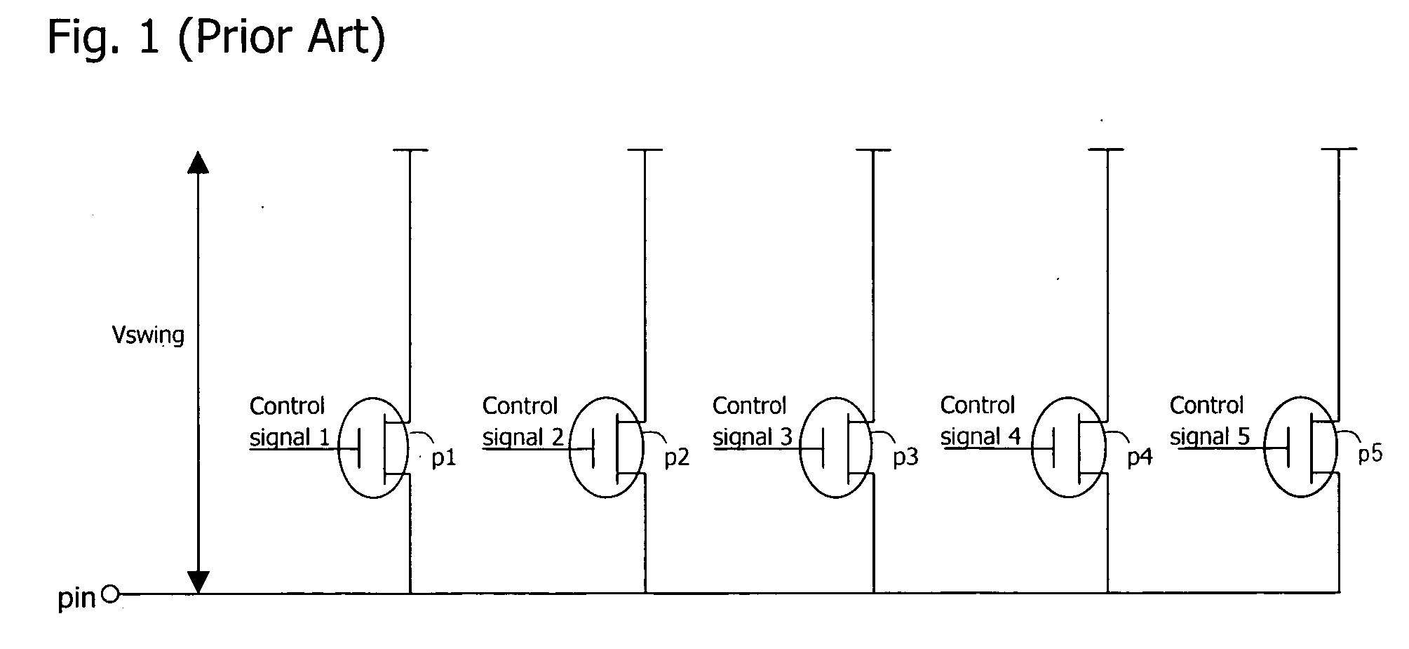
[0079] As shown in FIGS. 10A and 11A, the on-die termination circuit of the present embodiment includes: main resistance circuit A made up from transistor p1, which is a PMOS transistor, and resistance element r0; and adjustment circuit B which is made up from transistors p2˜p5, which are PMOS transistors, transistors p2˜p5 being both connected together in parallel and connected in parallel to main resistance circuit A.

[0080] One termi...

second embodiment

[0115]FIG. 13 shows the configuration of the on-die termination circuit of the second embodiment of the present invention.

[0116] As shown in FIG. 13, the on-die termination circuit of this embodiment differs from the first embodiment in that the termination voltage is changed from the power supply voltage VDD to GND, and transistors p1˜p5 are changed to transistors n1˜n5, which are NMOS transistors.

[0117] The present embodiment is also assumed to be of a binary configuration. If the width w of transistor n2 is assumed to be NW, the width w of each of transistors n3, n4, and n5 is NW / 2, NW / 4, and NW / 8, respectively.

third embodiment

[0118]FIG. 14 shows the configuration of the on-die termination circuit of the third embodiment of the present invention.

[0119] As shown in FIG. 14, the on-die termination circuit of this embodiment is a device in which a circuit whose termination voltage is the power supply voltage VDD, as in the first embodiment, and a circuit whose termination voltage is GND, as in the second embodiment, are associated by sharing the terminal pin. The termination voltage can thus be set to ½ of the level of power supply voltage VDD.

[0120] In addition, this embodiment is also assumed to be of a binary configuration, but the relation of the widths w of transistors p1˜p5 is the same as in the first embodiment and the relation of the widths of transistors n1˜n5 is the same as in the second embodiment.


PUM


Abstract

The on-die termination circuit of the present invention includes a main resistance circuit and an adjustment circuit. The main resistance circuit is provided with a resistance element and a transistor that is turned OFF when the on-die termination circuit is to be placed in the OFF state and turned ON when the on-die termination circuit is to be placed in the ON state. The adjustment circuit is provided with transistors that are both connected together in parallel and connected in parallel to the main resistance circuit, and that are turned ON or OFF when the on-die termination circuit is placed in the ON state so as to adjust the termination resistance of the entire on-die termination circuit.

Description

BACKGROUND OF THE INVENTION [0001] 1. Field of the Invention [0002] The present invention relates to an on-die termination circuit mounted as a termination circuit in LSI (Large Scale Integration). [0003] 2. Description of the Related Art [0004] In recent years, the demand for LSI having higher speeds, greater bandwidth operation, and lower power consumption continues to grow, and the transfer bus inside an LSI must therefore be treated as a high-speed transmission path. The demand for miniaturization of LSI is also growing, and with this demand comes a growing need for mounting on-die termination circuits as termination circuits for terminating the transfer bus to absorb reflection of bus signals transmitted in the transfer bus in the LSI. Recently, devices in which on-die termination circuits are mounted such as DDR2 SDRAM (Double Data Rate 2-Synchronous Dynamic Random Access Memory) are being manufactured. [0005] In an on-die termination circuit, the termination resistance, which...

Claims


Application Information

Patent Timeline
Patent Type & Authority Applications(United States)
IPC IPC(8): H03K19/003
CPCH04L25/0298
Inventor KOBAYASHI, SHOTARO
Owner LONGITUDE LICENSING LTD
Why Eureka
Try Eureka