
Photovoltaic apparatus including spherical semiconducting particles

Inactive Publication Date: 2006-08-24
SPHERAL SOLAR POWER
View PDF25 Cites 42 Cited by
  • Summary
  • Abstract
  • Description
  • Claims
  • Application Information

AI Technical Summary

Benefits of technology

[0011] An object of an aspect of the present invention is to provide a reliable, efficient photovoltaic apparatus that can be mass-produced while the amount of semiconductor material such as high-purity silicon that is used is less than that used in the prior art.
[0016] Since the photoelectric conversion elements are disposed in the respective recesses, intervals are formed in between, that is, their arrangement is not dense. However, the number of photoelectric conversion elements used is decreased, with the result that the amount of high-purity material (e.g., silicon) in the photoelectric conversion elements is reduced and the step of connecting the photoelectric conversion elements to the conductors of the support is made easier:
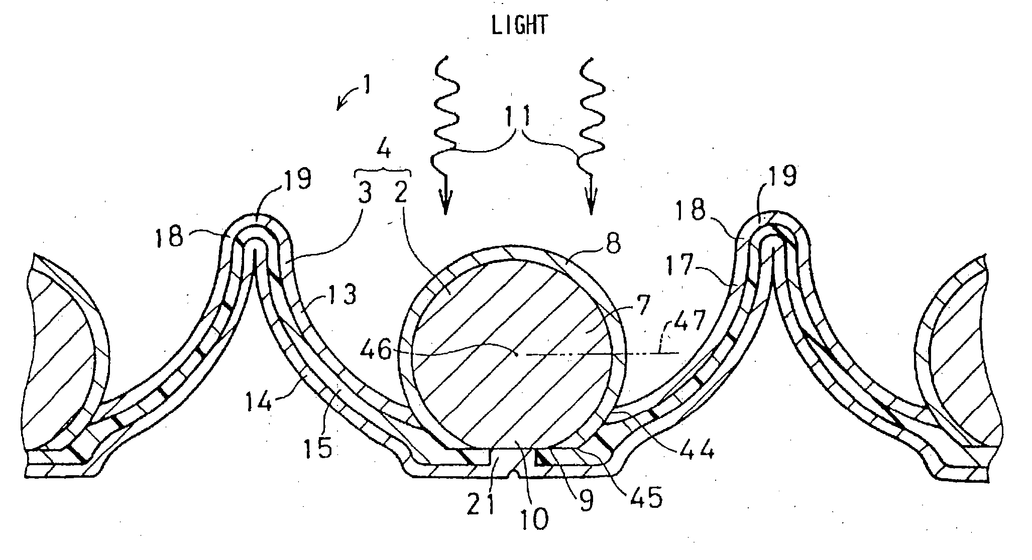
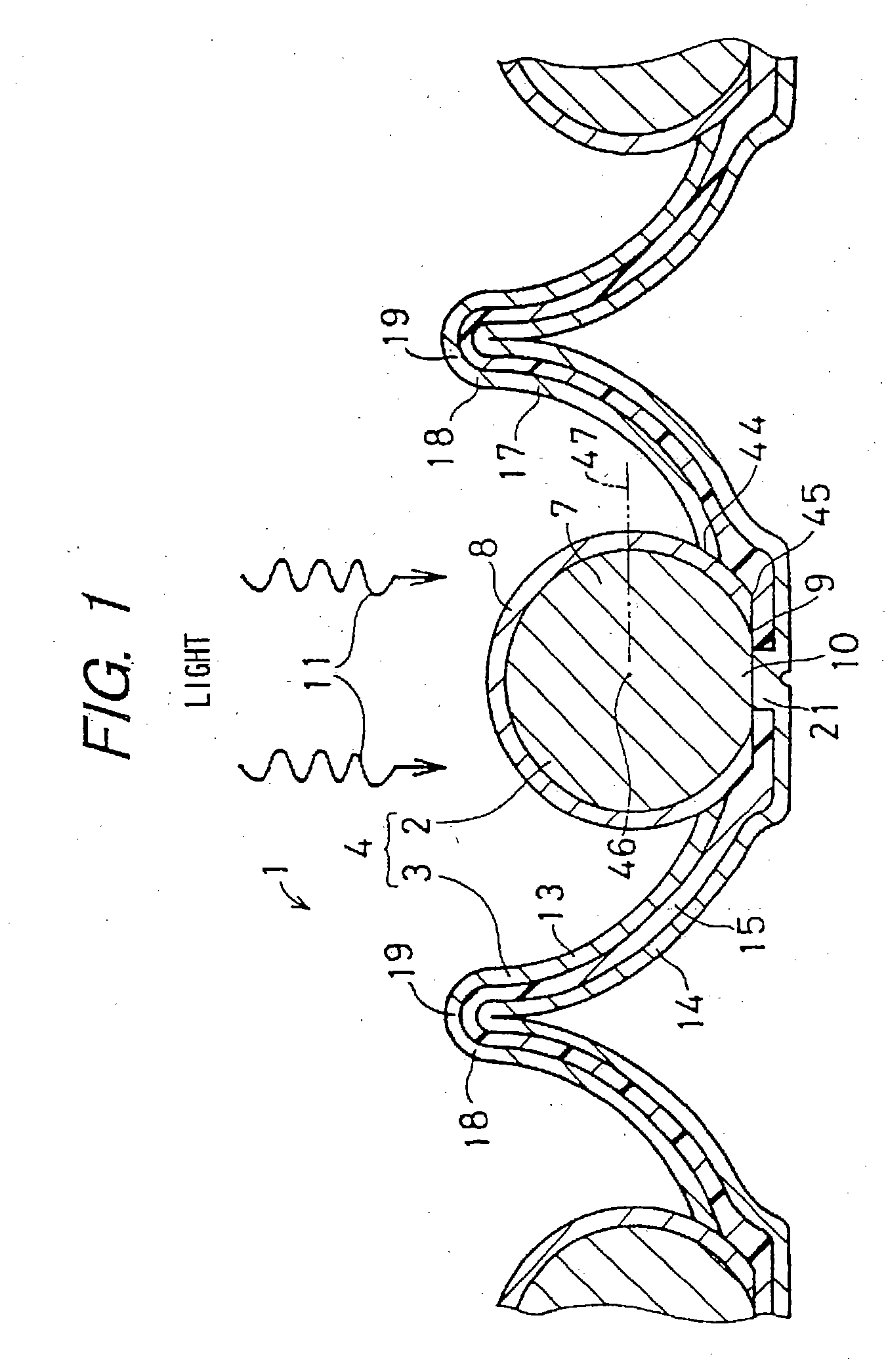
[0017] Further, the recesses are arranged adjacent to each other, whereby external light is reflected by the inside surfaces of the recesses and then applied to the photoelectric conversion elements. Therefore, external light is efficiently used for generation of photoelectromotive force by the photoelectric conversion elements.
[0026] In one aspect, shaped aluminum mesh foil forms a plurality of supports. Advantageously, the use of the shaped aluminum foil with substantially spherical photoelectric conversion elements reduces reflective losses of the spherical solar cell. Thus, the number of spheres used per unit area is reduced in comparison to prior-art structures producing comparable power. Thus, the amount of silicon used is reduced. Clearly, the overall power yield per kilogram of Si is improved.
[0030] The invention makes it possible to greatly reduce the used amount of photoelectric conversion element material (in particular, expensive silicon) and to simplify the step of connecting the photoelectric conversion elements to the support by decreasing the number of photoelectric conversion elements, to thereby increase the productivity and reduce the cost. In particular, the use of the photoelectric conversion elements according to the invention makes it possible to realize a manufacturing method capable of saving resources and energy. Sunlight or the like is reflected by the surface of the first conductor or a coating formed thereon that constitutes the inside surface of each recess of the support and resulting reflection light shines on the photoelectric conversion element. In this manner, incident light is utilized effectively. The first conductor or a coating formed thereon serves to not only reflect incident light but also guide currents (the first conductor is connected to the second semiconductor layers of the respective photoelectric conversion elements). Having a simple structure, the support is superior in productivity.

Problems solved by technology

This apparatus is costly because the production of a crystal is complex.
Furthermore, manufacturing a semiconductor wafer is not only complex because it includes cutting of a bulk single crystal, slicing, and polishing, but is also wasteful because crystal waste produced by the cutting, slicing, polishing etc. amounts to about 50% by volume or more of the original bulk single crystal.
The amorphous silicon photovoltaic apparatus, however, has a drawback in that the semiconductor has a number of crystal defects (i.e., gap states) inside the semiconductor due to the amorphous structure.
Also, the amorphous silicon solar battery suffers from the problem that the photoelectric conversion efficiency decreases due to a photo-induced deterioration phenomenon.
Even such a treatment, however, does not entirely eliminate the adverse effects of crystal defects.
It has become apparent that the degree of photo-induced deterioration decreases when the operation temperature of solar cells is high.
Although a module technique in which solar cells are caused to operate in such a condition is now being developed, it does not satisfy all the desired properties and further improvements are required.
This makes the connection of the particles to the sheets of aluminum foil complex, with the result that a sufficient cost reduction is not achieved.

Method used


Image

  • Photovoltaic apparatus including spherical semiconducting particles
  • Photovoltaic apparatus including spherical semiconducting particles
  • Photovoltaic apparatus including spherical semiconducting particles

Examples


Embodiment Construction

[0066] Now referring to the drawings, preferred embodiments of the invention are described below.

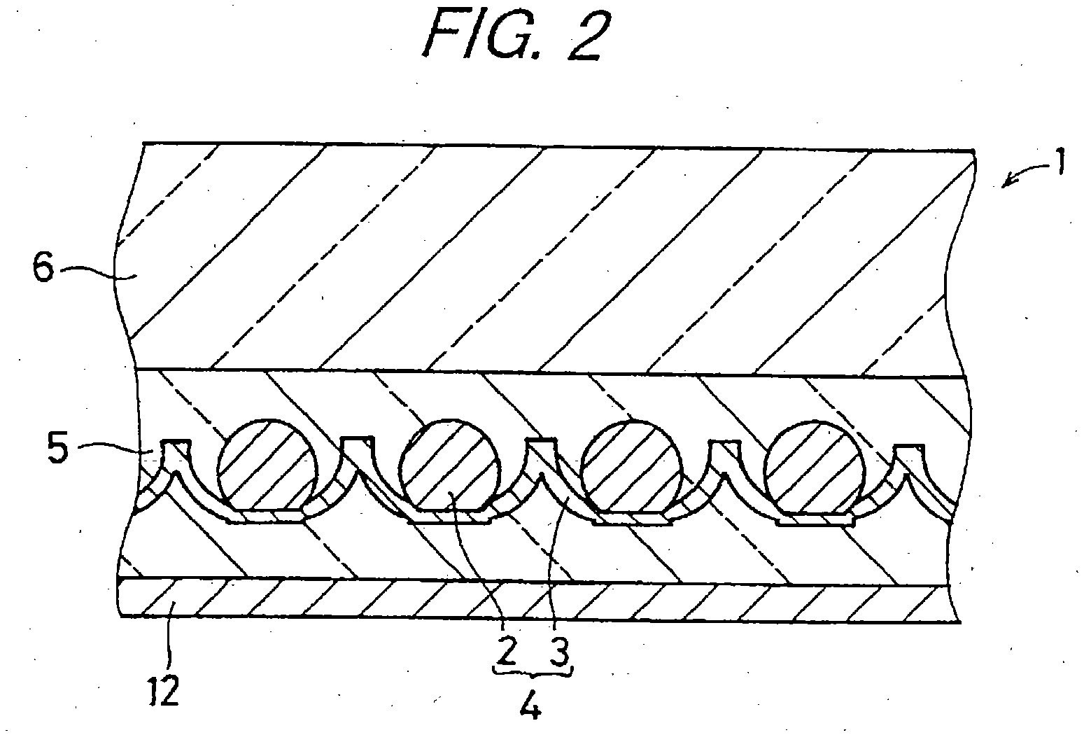
[0067]FIG. 1 is an enlarged sectional view of part of a photovoltaic apparatus 1 according to an embodiment of the present invention. FIG. 2 is a sectional view showing the structure of the photovoltaic apparatus 1. FIG. 3 is an exploded perspective view of the photovoltaic apparatus 1 of FIG. 2. The photovoltaic apparatus 1 has the following basic structure. An assembly 4 of a plurality of generally spherical photoelectric conversion elements 2 and a support 3 that is mounted with the photoelectric conversion elements 2 is buried in a filler layer 5 made of a transparent synthetic resin material such as PVB (poly(vinyl butyral)) or EVA (ethylene vinyl acetate). A transparent protective sheet 6 made of polycarbonate or the like is provided on the light source (e.g., sunlight) side of the filler layer 5 and is fixed to it. A waterproof back sheet 12 is fixed to the surface of the filler ...


PUM


Abstract

A photovoltaic apparatus includes a plurality of approximately spherical photoelectric conversion elements including a second semiconductor layer located outside a first semiconductor layer, for generating photoelectromotive force therebetween. The second semiconductor layer has an opening through which part of the first semiconductor layer is exposed. The apparatus also includes a support having first and second conductors and an insulator disposed between the conductors for electrically insulating the conductors from each other. The support has recesses adjacent to each other, the inside surfaces of which are constituted by the first conductor. The photoelectric conversion elements are disposed in respective recesses so that the elements are illuminated with light reflected by part of the first conductor that constitutes the recess. The first conductor is electrically connected to the second semiconductor layers of the photoelectric conversion elements, and the second conductor is electrically connected to the exposed portions of the first semiconductor layers.

Description

BACKGROUND OF THE INVENTION [0001] 1. Field of the Invention [0002] The present invention relates to a photovoltaic apparatus including substantially spherical semiconductor particles. [0003] In the disclosure herein described, the term “pin junction” is to be construed as including a structure that n-, l- and p-type semiconductor layers are formed on an approximately spherical photoelectric conversion element so as to be arranged in this order outward from the inside of the approximately spherical photoelectric conversion element or inward from the outside. [0004] 2. Description of the Related Art [0005] A typical photovoltaic apparatus comprises a photoelectric conversion element composed of a crystal silicon semiconductor wafer. This apparatus is costly because the production of a crystal is complex. Furthermore, manufacturing a semiconductor wafer is not only complex because it includes cutting of a bulk single crystal, slicing, and polishing, but is also wasteful because crysta...

Claims


Application Information

Patent Timeline
IPC IPC(8): H01L31/042
CPCH01L31/035281H01L31/03529Y02E10/50H01L31/048H01L31/0504H01L31/0547Y02E10/52
Inventor HAMMERBACHER, MILFRED DALEMATTHEWS, MARK DOUGLASS
Owner SPHERAL SOLAR POWER
Learn More