Method for assembling tiled detectors for ionizing radiation based image detection
- Summary
- Abstract
- Description
- Claims
- Application Information
AI Technical Summary
Benefits of technology
Problems solved by technology
Method used
Image
Examples
Embodiment Construction
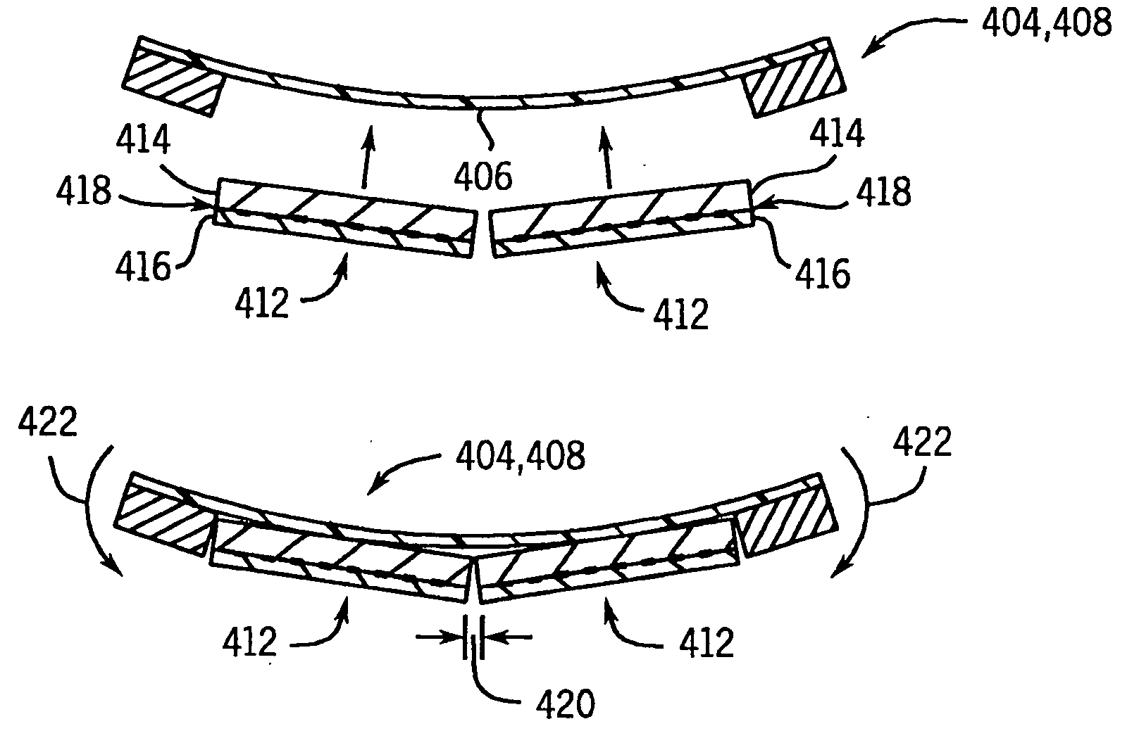
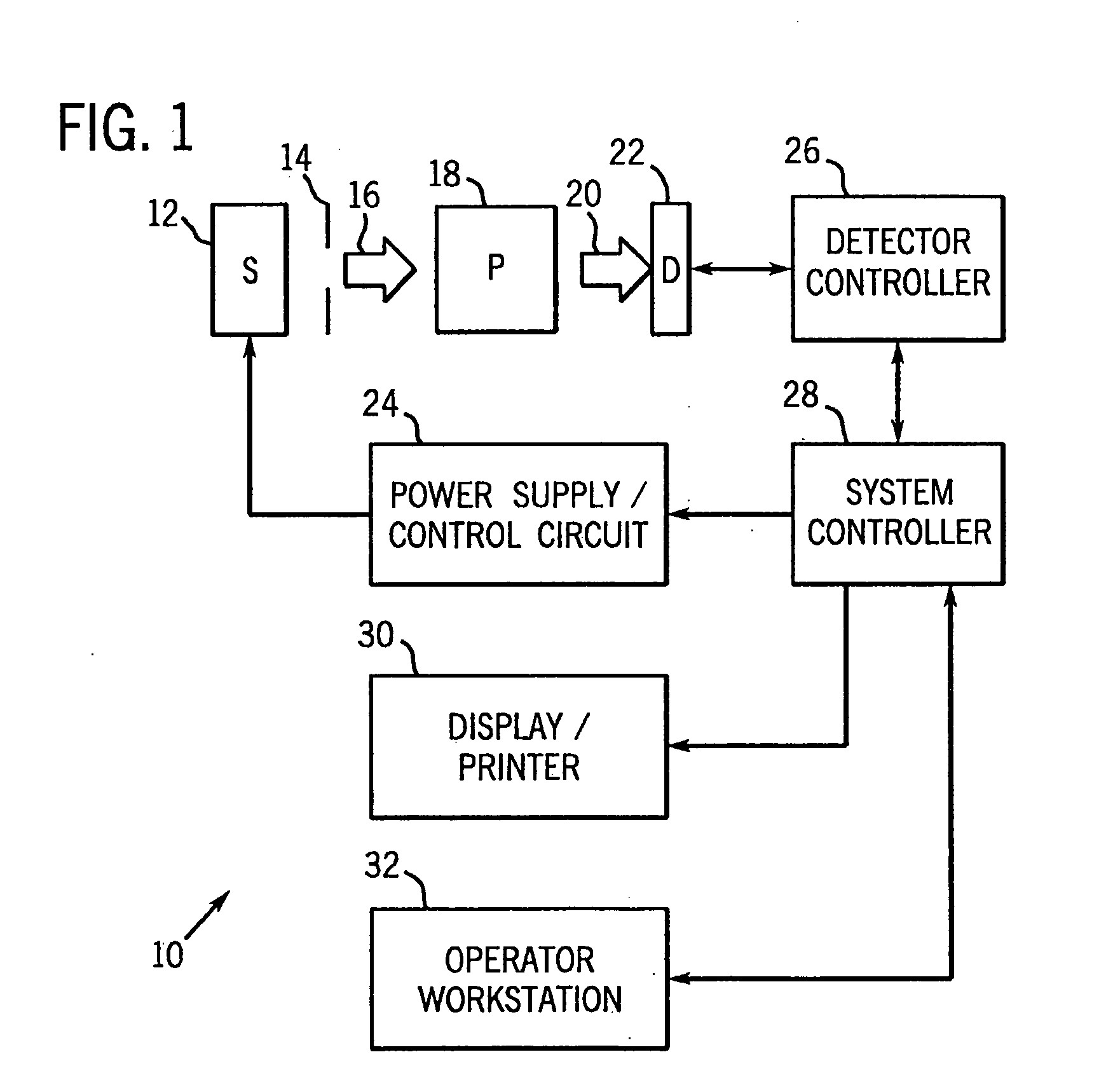
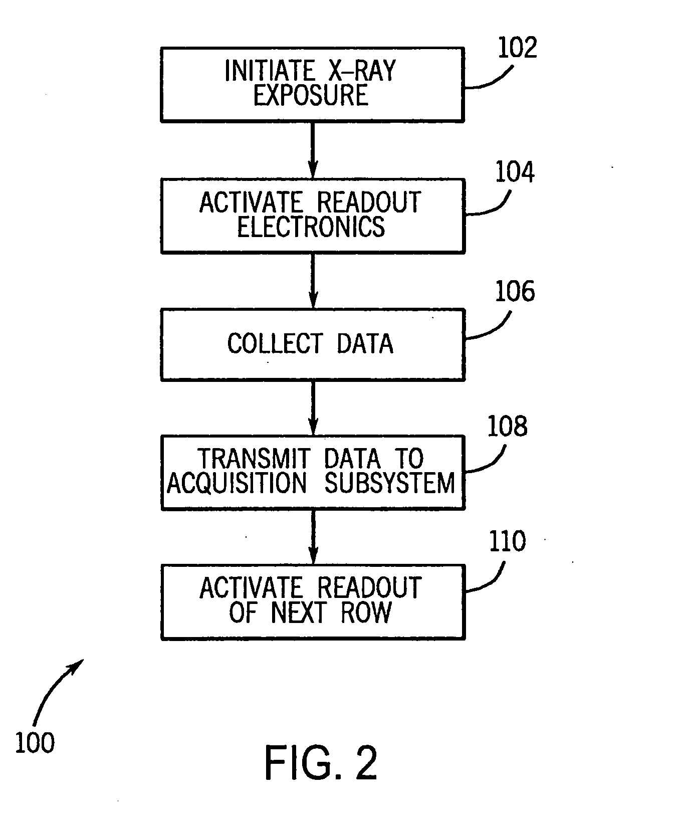
[0031] As described in detail below, the present technique relates to assembly and connection processes for imaging detectors made with multiple tiles of crystalline semiconductor material, such as Cadmium Zinc Telluride (CZT). However, the processes and detector assemblies described below are applicable to a wide variety of imaging systems, detector structures, and detector materials. For example, the present techniques are applicable to a variety of wide-bandgap semiconductors that may be used in direct conversion detectors for ionizing radiation, including CZT, Cadmium Telluride (CdTe), and Silicon CMOS. These assembly and connection processes produce imaging detectors having a plurality of tightly packed tiles and internally interconnected imaging layers, which may include ionizing photon detection layers, circuitry layers, and mechanical support layers. As follows, an exemplary imaging system is described with reference to FIGS. 1-2, followed by a detailed description of the fo...
PUM
| Property | Measurement | Unit |
|---|---|---|
| Temperature | aaaaa | aaaaa |
| Force | aaaaa | aaaaa |
| Flexibility | aaaaa | aaaaa |
Abstract
Description
Claims
Application Information
 - R&D
- Intellectual Property
- Life Sciences
- Materials
- Tech Scout
- Unparalleled Data Quality
- Higher Quality Content
- 60% Fewer Hallucinations
Browse by: Latest US Patents, China's latest patents, Technical Efficacy Thesaurus, Application Domain, Technology Topic, Popular Technical Reports.
© 2025 PatSnap. All rights reserved.Legal|Privacy policy|Modern Slavery Act Transparency Statement|Sitemap|About US| Contact US: help@patsnap.com


