Circuit for preventing simultaneous on operations
a technology of simultaneous operation and relay drive, which is applied in the direction of relays, manufacturing tools, pulse techniques, etc., can solve the problems of reducing the efficiency of ics structuring the inhibit circuit, the cost of b>4/b>, and the inability to prevent simultaneous operation, etc., to achieve the effect of improving the immunity against noise caused by static electricity, and low cos
- Summary
- Abstract
- Description
- Claims
- Application Information
AI Technical Summary
Benefits of technology
Problems solved by technology
Method used
Image

Examples
first embodiment
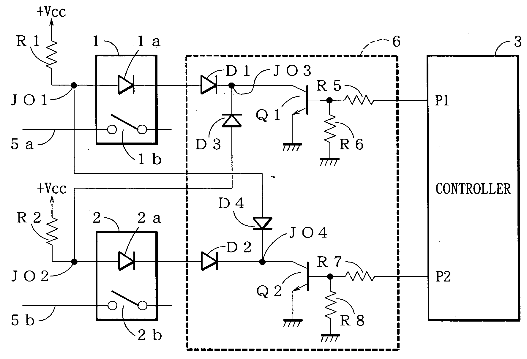
[0033]FIG. 1 is a circuit diagram showing a structure of a circuit for preventing simultaneous ON operations at a relay drive apparatus according to a first embodiment of the present invention.
[0034] In FIG. 1, a semiconductor relay drive circuit (relay drive apparatus) includes a controller 3 having two semiconductor relays (first and second relays) 1, 2 and a microcomputer for controlling ON / OFF operation of the semiconductor relays 1, 2. A circuit for preventing simultaneous ON operations 6 is connected between the semiconductor relays 1, 2 and control signal output terminals P1, P2 of the controller 3. The control signal output terminals P1, P2 output respectively control signals; one of those is “H” level and the other of those is “L” level.
[0035] The semiconductor relay 1 includes a photo-coupler having a light emitting diode 1a (first drive unit) connected through a first resistor R1 with +Vcc power supply and a semiconductor switch element (first switch device) 1b structur...
second embodiment
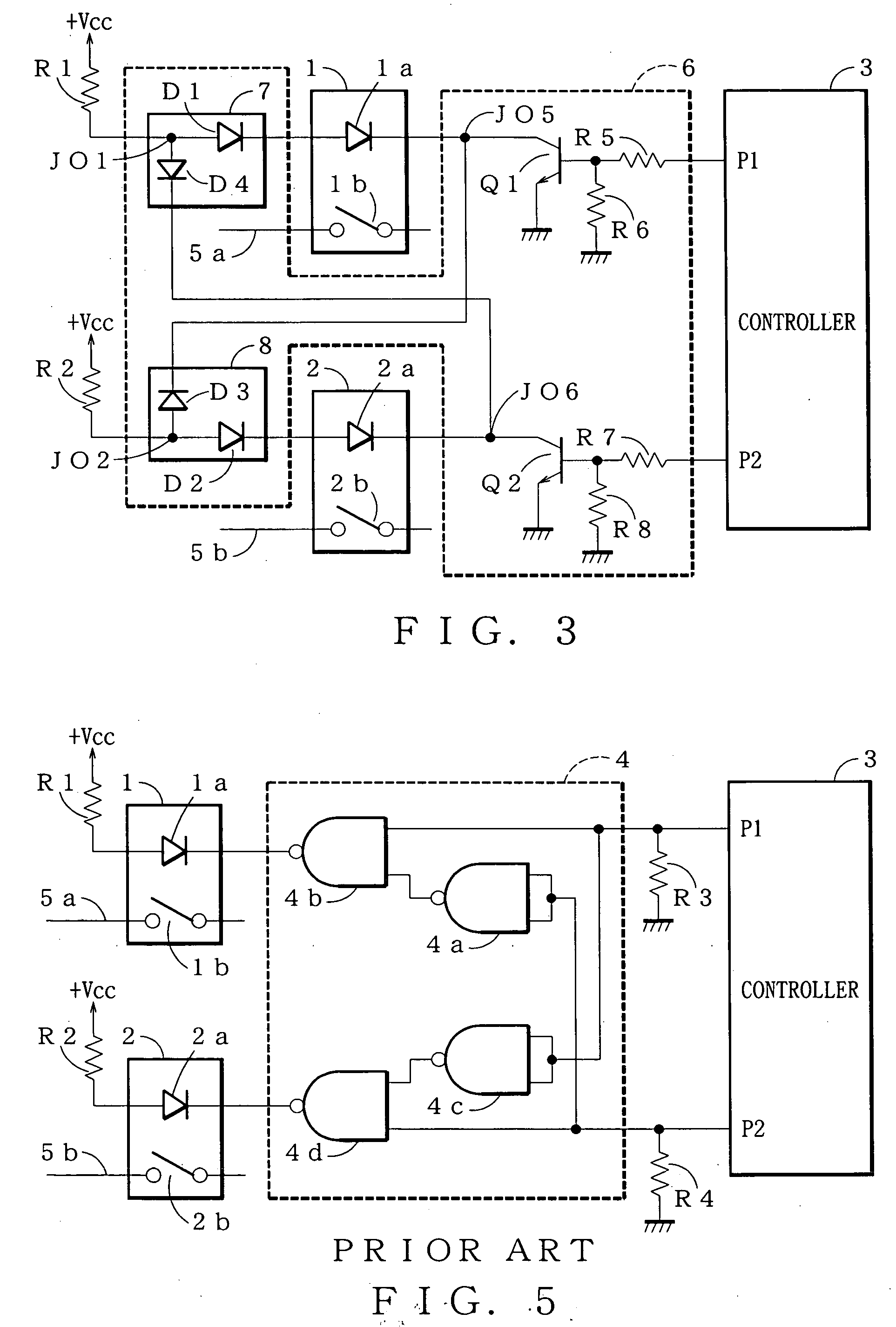
[0045]FIG. 3 is a circuit diagram showing a structure of a circuit for preventing simultaneous ON operations at a relay drive apparatus according to a second embodiment of the present invention.
[0046] In FIG. 3, a semiconductor relay drive circuit includes a controller 3 having two semiconductor relays 1, 2 and a microcomputer for controlling ON / OFF operation of the semiconductor relays 1, 2. A circuit for preventing simultaneous ON operations 6 is connected between the semiconductor relays 1, 2 and control signal output terminals P1, P2 of the controller 3. The control signal output terminals P1, P2 output respectively control signals; one of those is “H” level and the other of those is “L” level.
[0047] The semiconductor relay 1 includes a photo-coupler having a light emitting diode 1a connected through a first resistor R1 with +Vcc power supply and a semiconductor switch element 1b structured by a MOS-FET turning ON / OFF to be controlled by an output from the photo-coupler. The s...
third embodiment
[0058]FIG. 4 is a circuit diagram showing a structure of a circuit for preventing simultaneous ON operations at a relay drive apparatus according to a third embodiment of the present invention.
[0059] In FIG. 4, a semiconductor relay drive circuit includes a controller 3 having two semiconductor relays 1, 2 and a microcomputer for controlling ON / OFF operation of the semiconductor relays 1, 2. A circuit for preventing simultaneous ON operations 6 is connected between the semiconductor relays 1, 2 and control signal output terminals P1, P2 of the controller 3. The control signal output terminals P1, P2 output respectively control signals; one of those is “H” level and the other of those is “L” level.
[0060] The semiconductor relay 1 includes a photo-coupler having a light emitting diode 1a connected through a first resistor R1 with +Vcc power supply and a semiconductor switch element 1b structured by a MOS-FET turning ON / OFF to be controlled by an output from the photo-coupler. The se...
PUM
| Property | Measurement | Unit |
|---|---|---|
| drive current | aaaaa | aaaaa |
| OD | aaaaa | aaaaa |
| voltage | aaaaa | aaaaa |
Abstract
Description
Claims
Application Information
 - R&D
- Intellectual Property
- Life Sciences
- Materials
- Tech Scout
- Unparalleled Data Quality
- Higher Quality Content
- 60% Fewer Hallucinations
Browse by: Latest US Patents, China's latest patents, Technical Efficacy Thesaurus, Application Domain, Technology Topic, Popular Technical Reports.
© 2025 PatSnap. All rights reserved.Legal|Privacy policy|Modern Slavery Act Transparency Statement|Sitemap|About US| Contact US: help@patsnap.com