CMOS image sensor and fabricating method thereof
a technology of which is applied in the field of cmos image sensor and fabricating method thereof, can solve the problems of signal processing still limiting the corresponding area and the inability to maximize the photosensitivity, and achieve the effect of enhancing the light condensation
- Summary
- Abstract
- Description
- Claims
- Application Information
AI Technical Summary
Benefits of technology
Problems solved by technology
Method used
Image
Examples
Embodiment Construction
[0037] Reference will now be made in detail to embodiments of the present invention, examples of which are illustrated in the accompanying drawings. Wherever possible, the same reference designations will be used throughout the drawings to refer to the same or similar parts.
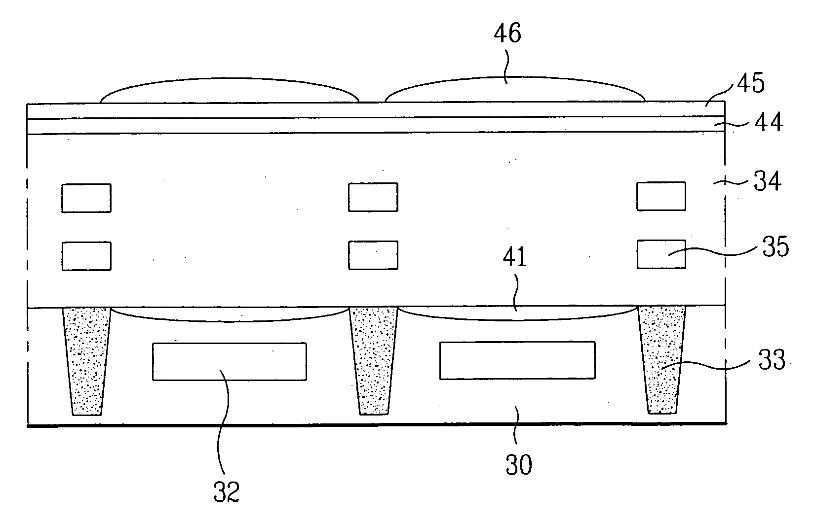
[0038] Referring to FIG. 2, a plurality of epitaxial layers (not shown) may be formed on a semiconductor substrate 30. A plurality of photodiodes are formed in a photodiode area 32. For example, a first epitaxial layer (not shown) may be grown on the semiconductor substrate 30, a red photodiode (not shown) may be formed on the first epitaxial layer, a second epitaxial layer (not shown) may be grown over the semiconductor substrate 30 including the red photodiode, and a green photodiode (not shown) may be then formed on the second epitaxial layer. Subsequently, a third epitaxial layer (not shown) may be grown on the second epitaxial layer including the green photodiode, a blue photodiode (not shown) may be formed...
PUM
 Abstract
Description
Claims
Application Information
 - R&D
- Intellectual Property
- Life Sciences
- Materials
- Tech Scout
- Unparalleled Data Quality
- Higher Quality Content
- 60% Fewer Hallucinations
Browse by: Latest US Patents, China's latest patents, Technical Efficacy Thesaurus, Application Domain, Technology Topic, Popular Technical Reports.
© 2025 PatSnap. All rights reserved.Legal|Privacy policy|Modern Slavery Act Transparency Statement|Sitemap|About US| Contact US: help@patsnap.com


