
Adjustable height wafer box

a height adjustment and wafer box technology, applied in the direction of damagable goods packaging, transportation and packaging, packaging types of goods, etc., can solve the problems of increasing shipping costs associated with it, and achieve the effect of reducing volumetric spa

Active Publication Date: 2006-07-06
ILLINOIS TOOL WORKS INC
View PDF8 Cites 12 Cited by
  • Summary
  • Abstract
  • Description
  • Claims
  • Application Information

AI Technical Summary

Benefits of technology

The present invention provides a box for semiconductor wafers that can be adjusted in size to reduce the space required for shipping partial lots of wafers. The box has a base plate, ring insert plates, and a cover plate, with the wall height being adjusted by adding or removing ring insert plates. The ring insert plates have notches to hold elastomer bumpers to protect the wafers. The inner diameter of the ring insert plates is chosen to accommodate the desired size of the wafers, with allowance for the elastomer bumpers. This allows for efficient use of space when shipping semiconductor wafers.

Problems solved by technology

This can increase the shipping costs associated with a “partial run” which is typically defined as less than twenty-four wafers.

Method used


Image

  • Adjustable height wafer box
  • Adjustable height wafer box
  • Adjustable height wafer box

Examples


Embodiment Construction

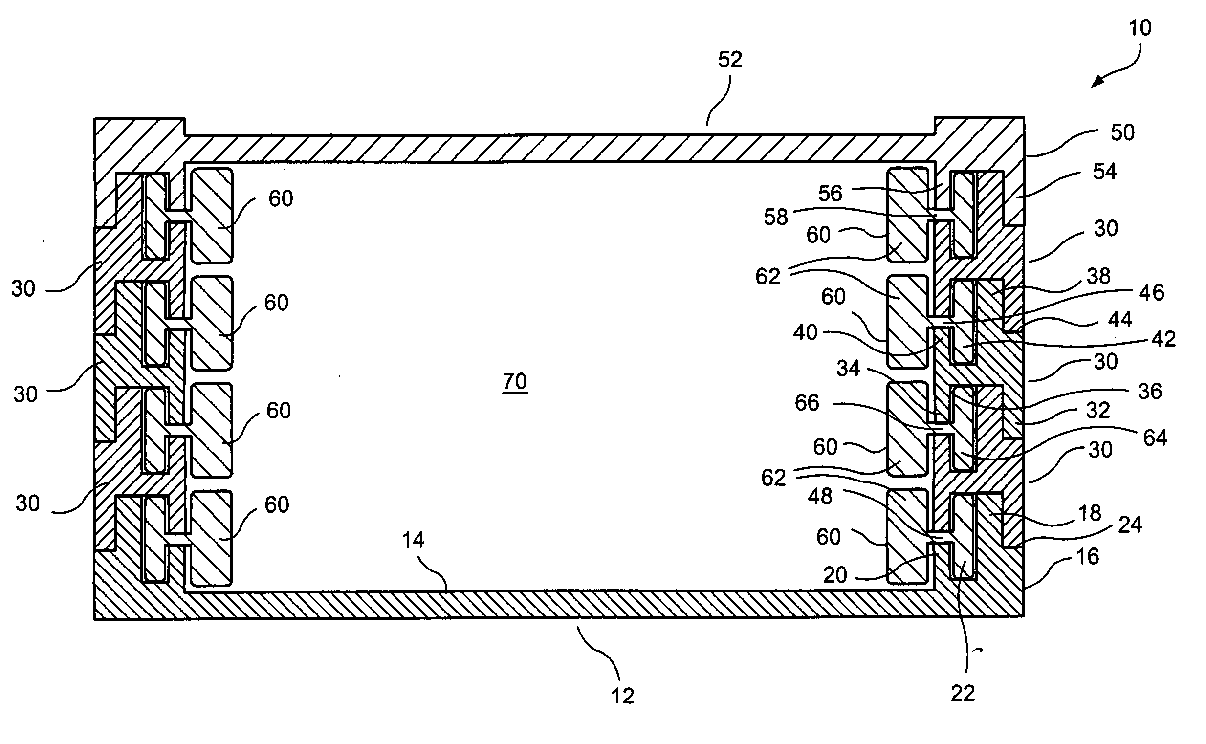
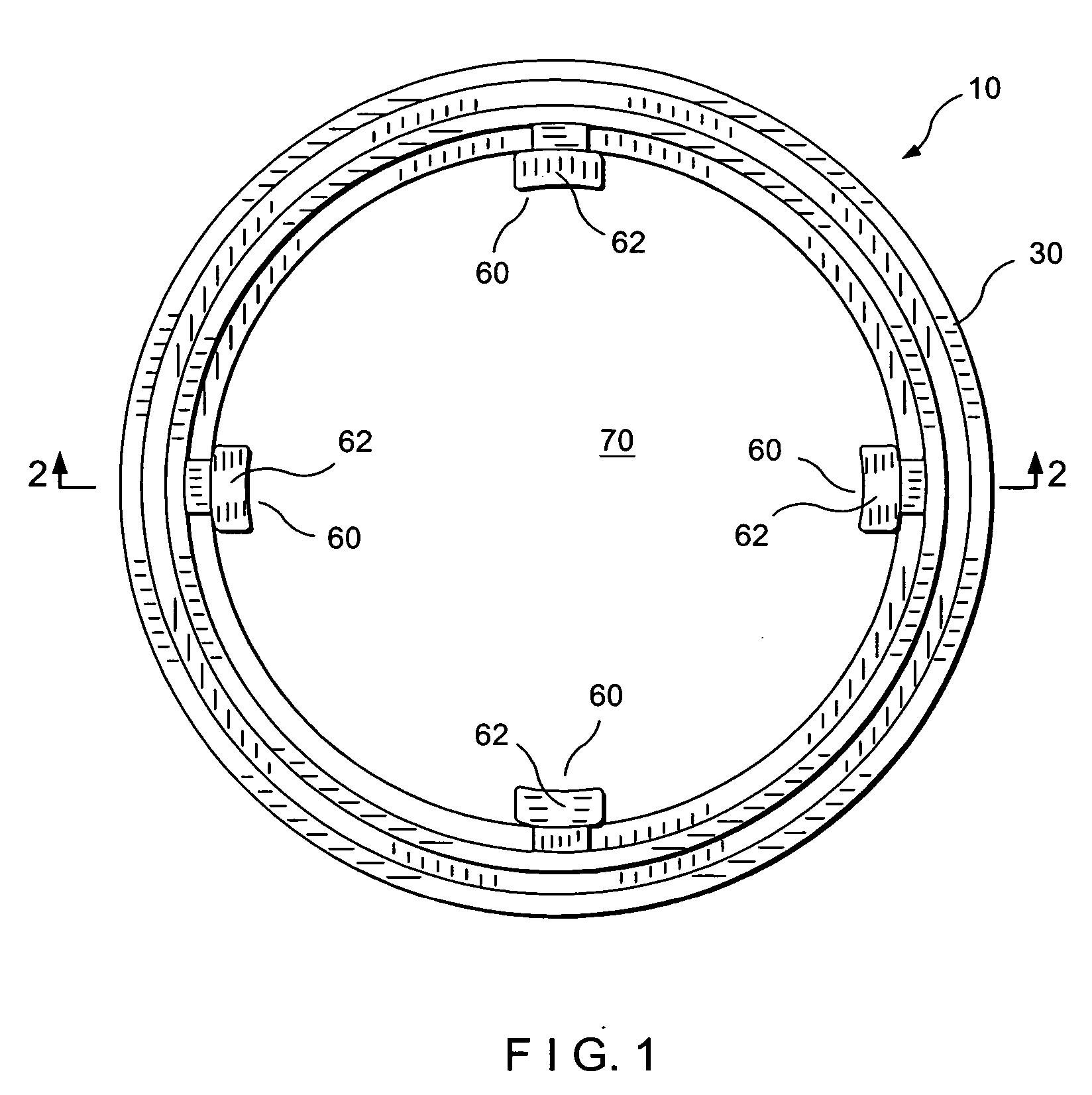
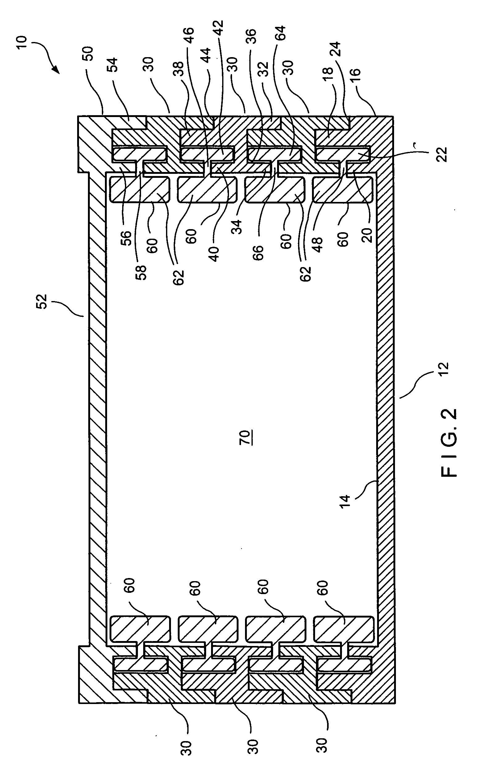
[0014] Referring now to the drawings in detail, wherein like numerals refer to like elements throughout the several views, one sees that FIG. 1 is a top plan view of the adjustable height wafer box 10 of the present invention (with the cover plate removed) and that FIG. 2 is a cross-sectional view of the adjustable height wafer box 10 of the present invention. Adjustable height wafer box 10 includes base plate 12, ring insert plates 30, cover plate 50 and elastomer bumpers 60. Wafer containment space 70 is formed within adjustable height wafer box 10. A typical material for the base plate 12, ring insert plates 30 and cover plate 50 is polyethylene plastic and a typical material for elastomer bumpers 60 is extruded soft or semi-soft plastic, but those skilled in the art will recognize a range of equivalents after review of this disclosure.

[0015] Base plate 12 comprises planar floor 14, outer cylindrical wall 16, upper circular ridge 18 recessed from outer cylindrical wall 16, and i...


PUM


Abstract

An adjustable height wafer box for the transportation of coin-stacked semiconductor wafers is disclosed. The adjustable height wafer box comprises a base plate, a cover plate, a plurality of ring insert plates and elastomer bumpers. The ring insert plates are stacked so as to successively engage one another, as well as engaging the base plate and the cover plate. The elastomer bumpers are engaged between successive ring insert plates and extend inwardly into the wafer containment space. The number of ring insert plates can be chosen to adjust the height of the wafer box in accordance with the number of coin-stacked semiconductor wafers to be shipped.

Description

BACKGROUND OF THE INVENTION [0001] 1. Field of the Invention [0002] This invention pertains to a box for the transportation of semiconductor wafers. In particular, this invention pertains to such a box with walls that are adjustable in height so as to accommodate the number of coin-stacked wafers to be transported. [0003] 2. Description of the Prior Art [0004] In the prior art, there are many boxes for the transportation of coin-stacked semiconductor wafers. However, typical prior art wafer boxes have a fixed size for a fixed number of semiconductor wafers. As a result, the volume of shipping containers and dunnage material is the same regardless of the number of wafers enclosed within the wafer box. This can increase the shipping costs associated with a “partial run” which is typically defined as less than twenty-four wafers. [0005] Examples of some prior art are U.S. Pat. No. 6,193,068 entitled “Containment Device for Retaining Semiconductor Wafers” issued on Feb. 27, 2001 to Lewi...

Claims


Application Information

Patent Timeline
Patent Type & Authority Applications(United States)
IPC IPC(8): B65D85/30
CPCH01L21/67346H01L21/67386
Inventor FORSYTH, VALORIS L.
Owner ILLINOIS TOOL WORKS INC
Learn More