Symmetric optical modulator with low driving voltage
a technology of symmetric optical modulators and driving voltages, applied in optics, instruments, optical light guides, etc., can solve the problems of low driving voltage, high driving voltage, and insignificant difference in modulators, and achieve low voltage driving and no signal distortion
- Summary
- Abstract
- Description
- Claims
- Application Information
AI Technical Summary
Benefits of technology
Problems solved by technology
Method used
Image
Examples
first embodiment
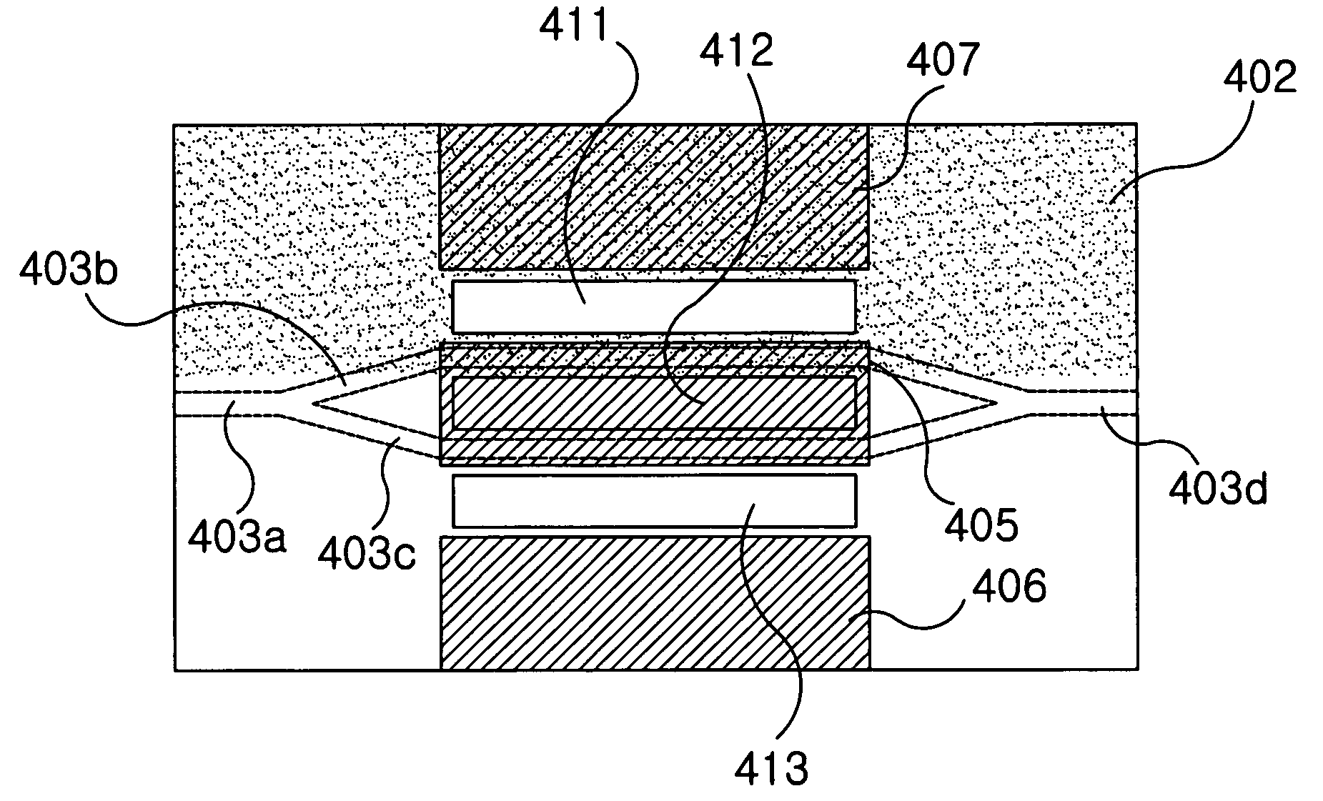
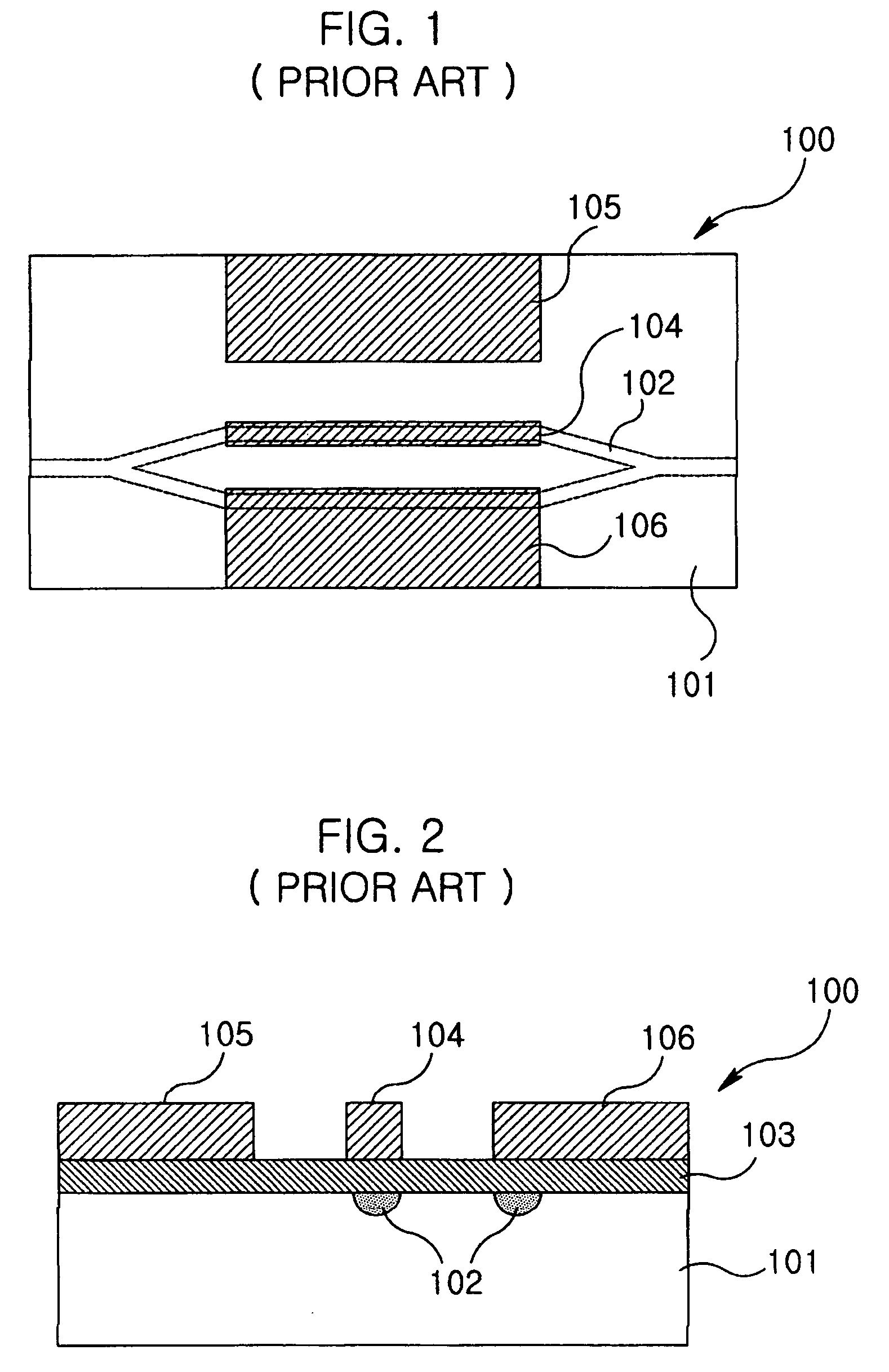
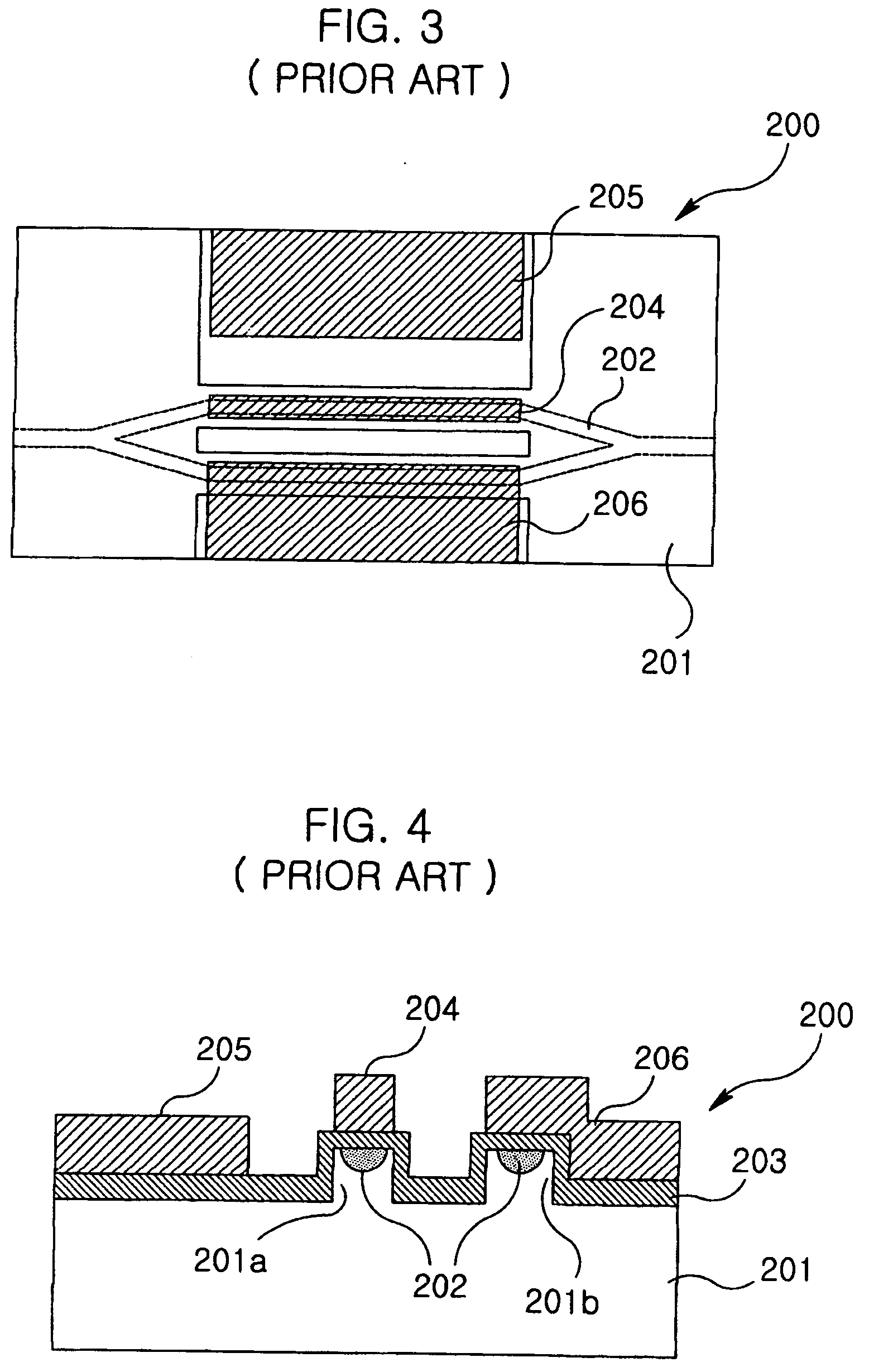
[0067]FIG. 12 is a schematic sectional view of a first embodiment according to the present invention. The symmetric optical modulator with low driving voltage according to the present invention includes a substrate (401); an optical waveguide composed of an input portion (403a), a pair of first and second branch portions (403b, 403c) branched off from the input portion (403a), and an output portion (403d) where the first and second branch portions (403b, 403c) are combined, all of which being formed inwardly on a top surface of the substrate (401); a polarization inversion region (402) corresponding to a region of the substrate (401) delimited by the first or second branch portion (403b, 403c) of the optical waveguide; first to third grooves (411, 412, 413) formed by etching portions of the substrate (401) adjacent to the sides of the first and second branch portions (403b, 403c) of the optical waveguide; a buffer layer (404) formed on the top surface of the substrate (401) includin...
second embodiment
[0068]FIG. 13 is a schematic sectional view of a second embodiment according to the present invention. The symmetric optical modulator with low driving voltage according to the present invention includes a substrate (401); an optical waveguide composed of an input portion (403a), a pair of first and second branch portions (403b, 403c) branched off from the input portion (403a), and an output portion (403d) where the first and second branch portions (403b, 403c) are combined, all of which being formed inwardly on a top surface of the substrate (401); a polarization inversion region (402) corresponding to a region of the substrate (401) delimited by the first or second branch portion (403b, 403c) of the optical waveguide; first to third grooves (411, 412, 413) formed by etching portions of the substrate (401) adjacent to the sides of the first and second branch portions (403b, 403c) of the optical waveguide; a buffer layer (404) formed on a top surface of the first and second branch p...
PUM
| Property | Measurement | Unit |
|---|---|---|
| impedance | aaaaa | aaaaa |
| thickness | aaaaa | aaaaa |
| thickness | aaaaa | aaaaa |
Abstract
Description
Claims
Application Information
 - R&D
- Intellectual Property
- Life Sciences
- Materials
- Tech Scout
- Unparalleled Data Quality
- Higher Quality Content
- 60% Fewer Hallucinations
Browse by: Latest US Patents, China's latest patents, Technical Efficacy Thesaurus, Application Domain, Technology Topic, Popular Technical Reports.
© 2025 PatSnap. All rights reserved.Legal|Privacy policy|Modern Slavery Act Transparency Statement|Sitemap|About US| Contact US: help@patsnap.com


