Printed circuit board including embedded capacitor and method of fabricating same

a technology of printed circuit boards and capacitors, applied in the field of printed circuit boards, can solve problems such as poor electric performance of electronic goods, and achieve the effect of preventing the occurrence of parasitic inductan

Inactive Publication Date: 2006-06-01
SAMSUNG ELECTRO MECHANICS CO LTD
View PDF20 Cites 5 Cited by
  • Summary
  • Abstract
  • Description
  • Claims
  • Application Information

AI Technical Summary

Benefits of technology

[0031] Another object of the present invention is to provide a PCB including an embedded capacitor, in which an unnecessary portion of a lower electrode layer is not formed, thereby preventing the occurrence of parasitic inductance, and a method of fabricating the same.

Problems solved by technology

The protrusion of the lower electrode layer 12a acts as a conductor in a high frequency environment, causing parasitic inductance, resulting in poor electric performance of electronic goods.

Method used


Image

  • Printed circuit board including embedded capacitor and method of fabricating same
  • Printed circuit board including embedded capacitor and method of fabricating same
  • Printed circuit board including embedded capacitor and method of fabricating same

Examples


Embodiment Construction

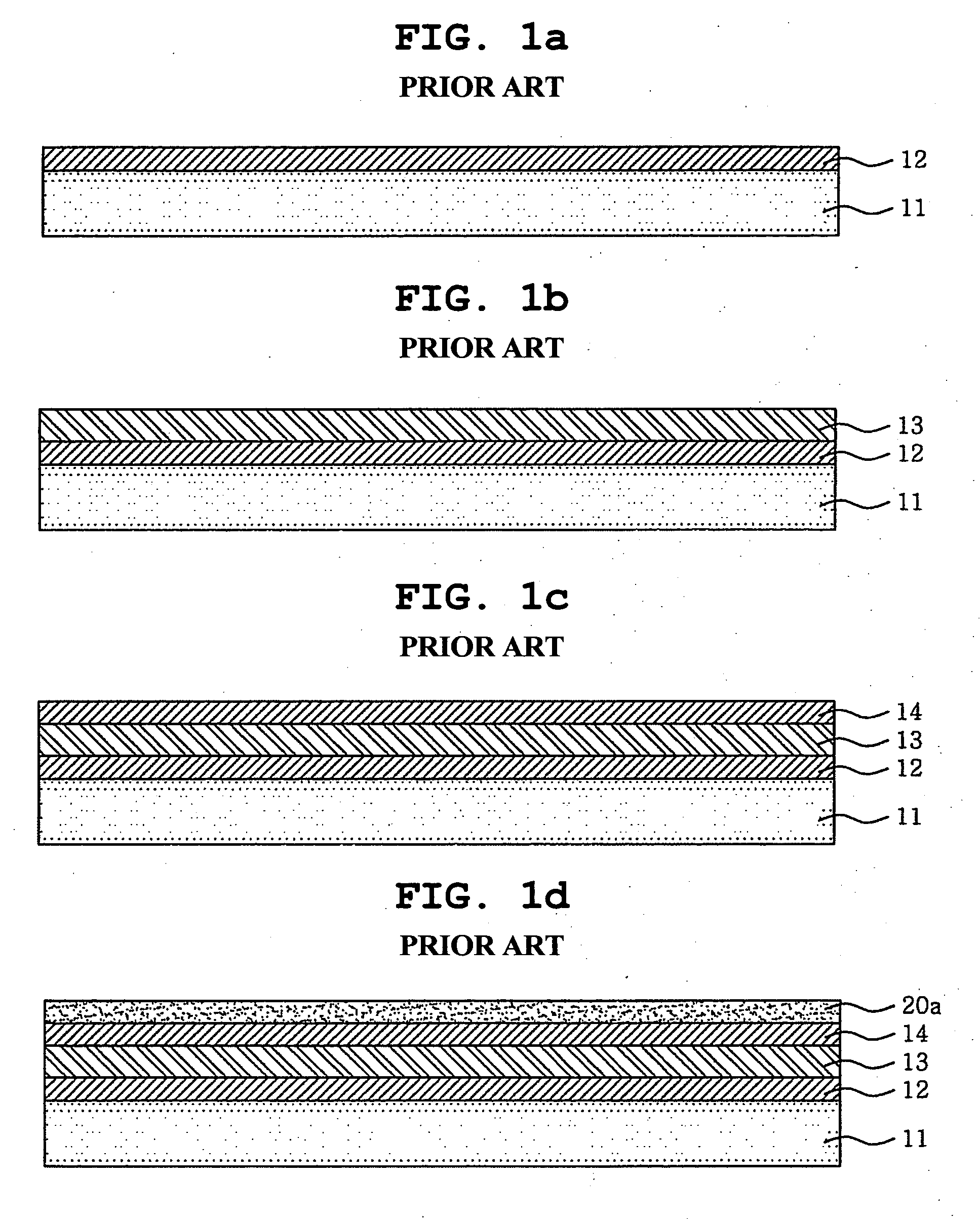
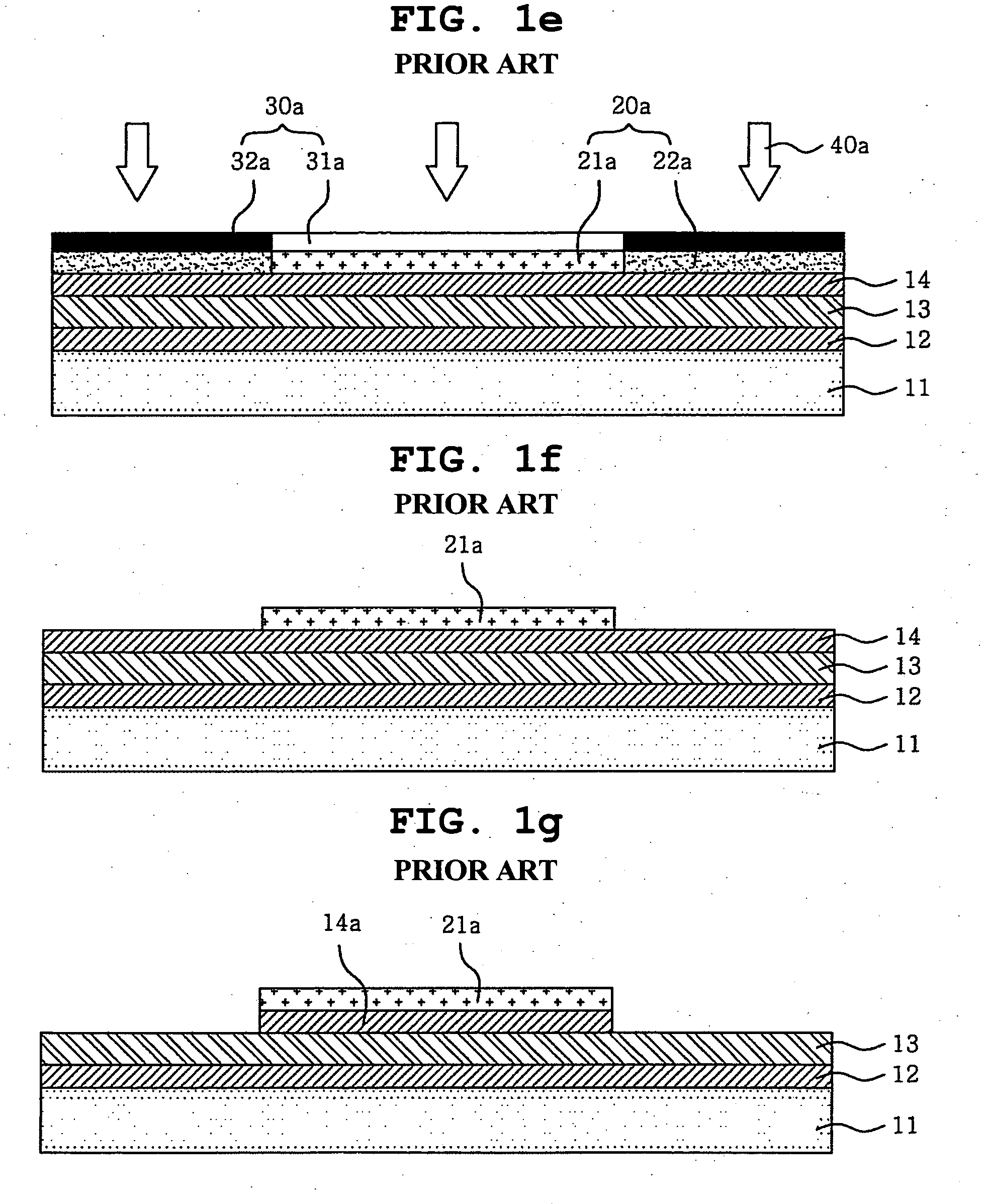
[0043] Hereinafter, a detailed description will be given of a PCB including an embedded capacitor and a method of fabricating the same according to the present invention, with reference to the drawings. In the drawings of the present invention, only one side of the PCB is processed, but both sides of the PCB are processed in practice.

[0044]FIG. 3 is a sectional view of a PCB including an embedded capacitor, according to an embodiment of the present invention.

[0045] As shown in FIG. 3, the PCB 100 including the embedded capacitor according to the present invention comprises an insulating layer 111, a lower electrode layer 112a and a circuit pattern 112b formed on the insulating layer 111, a dielectric layer 113a formed on the lower electrode layer 112a, an upper electrode layer 114a formed on the dielectric layer 113a, and an insulating resin 115 packed between the lower electrode layer 112a and the circuit pattern 112b.

[0046] The insulating layer 111 is interposed between circuit...


PUM

PropertyMeasurementUnit
widthaaaaaaaaaa
photosensitiveaaaaaaaaaa
sizeaaaaaaaaaa

Abstract

Disclosed is a PCB including an embedded capacitor, in which a dielectric layer and an upper electrode layer are formed after a lower electrode layer of the embedded capacitor is formed, thereby providing a microcircuit pattern on a circuit layer having a lower electrode layer formed thereon, and a method of fabricating the same.

Description

INCORPORATION BY REFERENCE [0001] The present application claims priority under 35 U.S.C. §119 to Korean Patent Application No. 2004-99898 filed on Dec. 1, 2004. The content of the application is incorporated herein by reference in its entirety. BACKGROUND OF THE INVENTION [0002] 1. Field of the Invention [0003] The present invention relates, in general, to a printed circuit board (PCB) including an embedded capacitor and a method of fabricating the same and, more particularly, to a PCB including an embedded capacitor, in which a dielectric layer and an upper electrode layer are formed after a lower electrode layer of the embedded capacitor is formed, thereby providing a microcircuit pattern on a circuit layer having the lower electrode layer formed thereon, and a method of fabricating the same. [0004] 2. Description of the Prior Art [0005] Recently, electronic technologies are moving toward the embedding of resistors, capacitors, integrated circuits (IC) and the like into a substra...

Claims


Application Information

Patent Timeline
Patent Type & Authority Applications(United States)
IPC IPC(8): G03C5/00
CPCH05K1/162H05K3/0023H05K3/0082H05K3/064H05K3/108H05K3/181H05K3/184H05K3/4644H05K2201/0355H05K2201/09509H05K2201/09881H05K2203/0551H05K1/16
Inventor HONG, JONG KUKRYU, CHANG SUPJEON, HO SIKLEE, SEOK KYU
Owner SAMSUNG ELECTRO MECHANICS CO LTD
Why Eureka
Try Eureka