
High performance, low leakage SRAM device and a method of placing a portion of memory cells of an SRAM device in an active mode

a memory cell and active mode technology, applied in static storage, digital storage, instruments, etc., can solve the problems of inability to write, low leakage rate, and inability to access data of a sram device in a standby mode, so as to improve the access time of the sram, reduce the capacitance of the bitline, and high performance access

Active Publication Date: 2006-05-11
TEXAS INSTR INC
View PDF12 Cites 20 Cited by
  • Summary
  • Abstract
  • Description
  • Claims
  • Application Information

AI Technical Summary

Benefits of technology

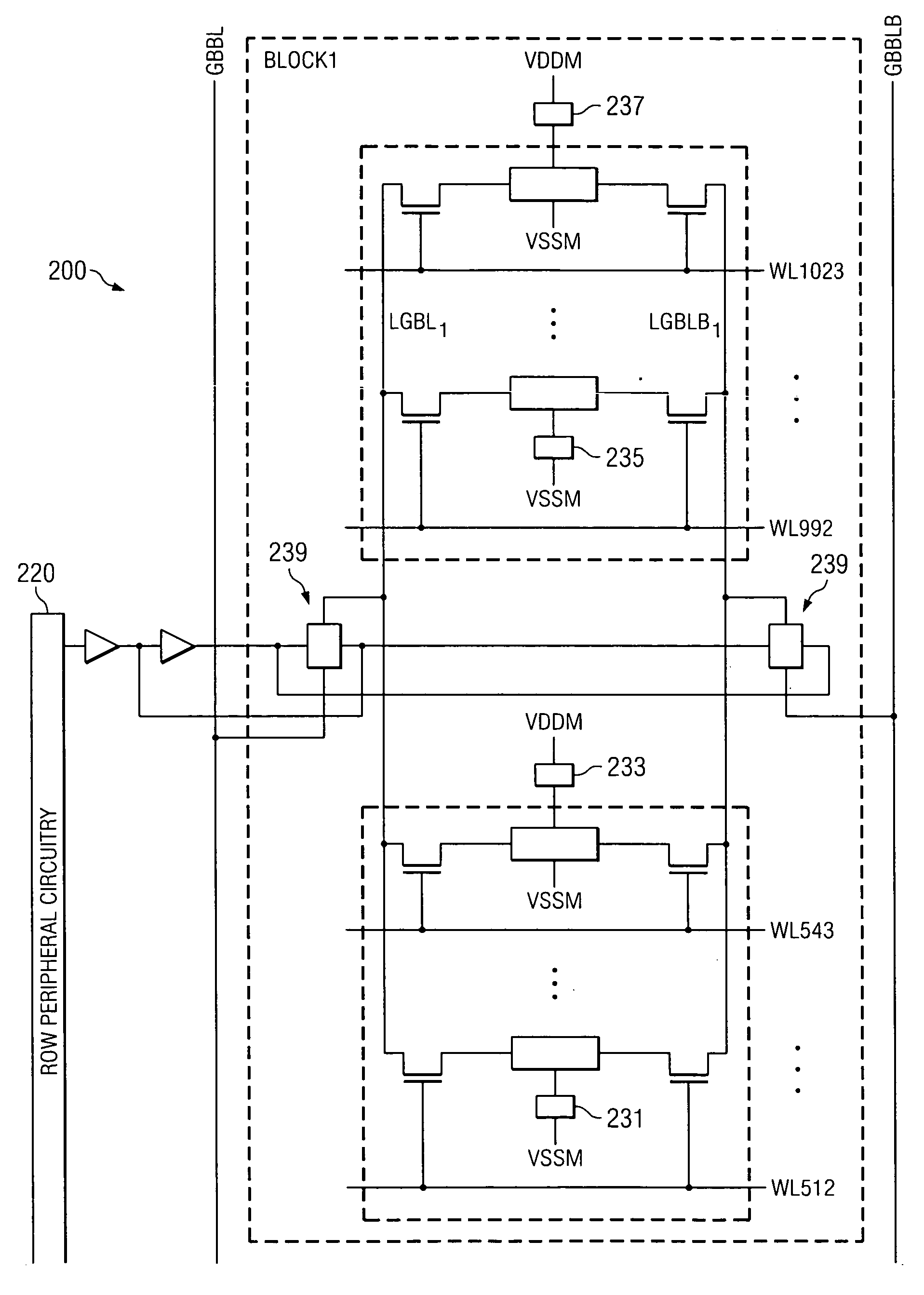
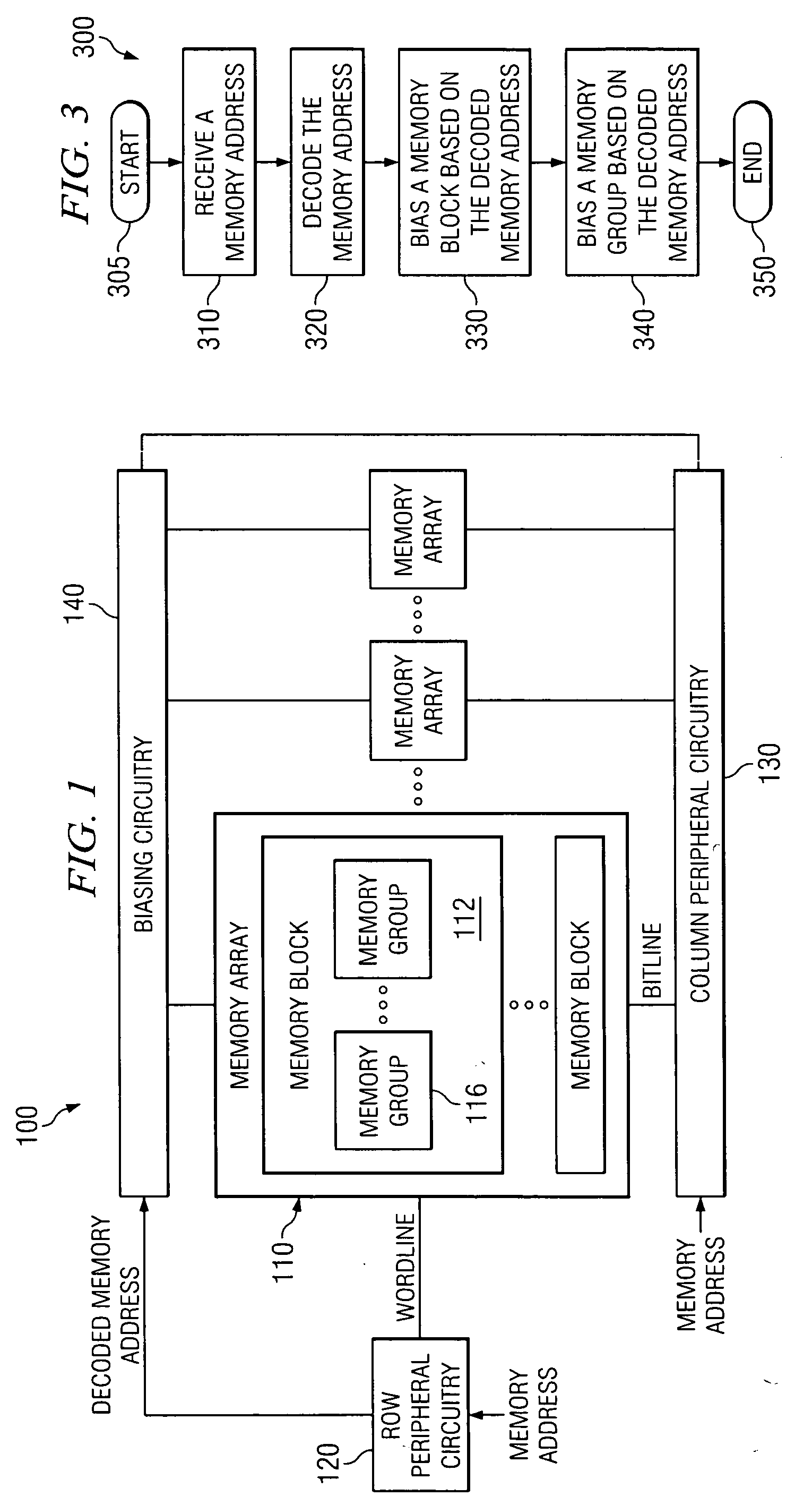
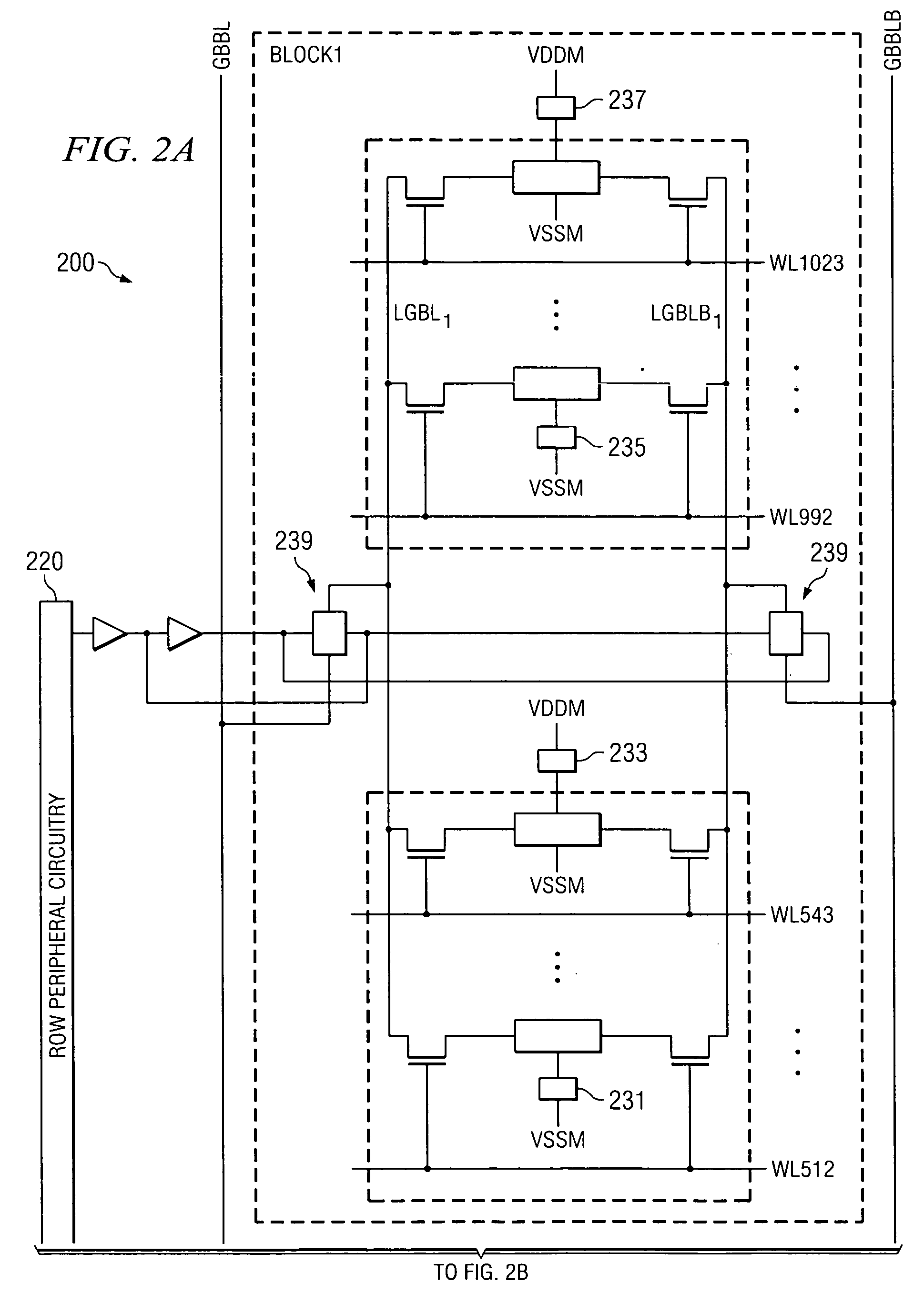
[0010] The present invention provides a low-leakage active mode SRAM for high performance access with flexible hierarchical grouping of the memory cells. The hierarchical grouping advantageously divides the SRAM device at least into sets and subsets of memory cells to reduce bitline capacitance and, thus, improve access time for the SRAM. The biasing circuitry advantageously employs a decoded memory address signal to selectively bias sets and subsets of memory cells.

Problems solved by technology

ROM, however, does not accommodate writing.
SRAM devices, however, are often employed within battery-powered wireless apparatus where power consumption is an important design parameter.
As transistor size continues to diminish (e.g., 90 nm transistors), current leakage may be unacceptably high even during standby mode, requiring a transition to a still lower power consumption level, a data retention or sleep mode, to conserve power adequately.
Accessing data of a SRAM device in a standby mode, however, suffers due to time and energy required to transition from the standby mode to an active mode.

Method used


Image

  • High performance, low leakage SRAM device and a method of placing a portion of memory cells of an SRAM device in an active mode
  • High performance, low leakage SRAM device and a method of placing a portion of memory cells of an SRAM device in an active mode
  • High performance, low leakage SRAM device and a method of placing a portion of memory cells of an SRAM device in an active mode

Examples


Embodiment Construction

[0018] Referring initially to FIG. 1, illustrated is a block diagram of an embodiment of an SRAM device, generally designated 100, constructed according to the principles of the present invention. The SRAM device 100 includes a plurality of memory arrays, row peripheral circuitry 120, main column peripheral circuitry 130 and biasing circuitry 140. One memory array of the plurality of memory arrays, memory array 110, is selected to represent each of the plurality of memory arrays.

[0019] The memory array 110 includes multiple memory cells organized in a matrix of columns and rows. The memory cells of the memory array 110 are configured into sets denoted as memory blocks and represented by memory block 112. Additionally, the memory cells in memory block 112 are configured into subsets denoted as memory groups and represented by memory group 116. One skilled in the art will understand that the memory array 110, the memory block 112 or the memory group 116 may be considered as a set of ...


PUM


Abstract

An SRAM device a method of placing a portion of memory cells of an SRAM device in an active mode. In one embodiment, the SRAM device includes (1) a set of memory cells and (2) biasing circuitry, coupled to the set, configured to bias a subset of the set based on a memory address associated therewith.

Description

TECHNICAL FIELD OF THE INVENTION [0001] The present invention is directed, in general, to memory devices and, more specifically, to a Static Random-Access Memory an SRAM device in an active mode. BACKGROUND OF THE INVENTION [0002] Different types of memory are used in electronic apparatus for various purposes. Read-Only Memory (ROM) and Random Access Memory (RAM) are two such types of memory commonly used within computers for different memory functions. ROM retains its stored data when power is switched off and therefore is often employed to store programs that are needed for initializing (colloquially, “booting up”) an apparatus. ROM, however, does not accommodate writing. RAM, on the other hand, allows data to be written to or read from selected addresses associated with memory cells and, therefore, is typically used during normal operation of the apparatus. [0003] Two common types of RAM are dynamic RAM (DRAM) and static RAM (SRAM). DRAM is typically used for the main memory of c...

Claims


Application Information

Patent Timeline
IPC IPC(8): G11C11/00G11C5/14
CPCG11C7/12G11C8/12G11C11/413
Inventor DANG, LUANTRAN, HIEP VAN
Owner TEXAS INSTR INC
Learn More