Apparatus and methods for saving power and reducing noise in integrated circuits
a technology of integrated circuits and apparatus, applied in the field of apparatus and methods for saving power and reducing noise in integrated circuits, can solve the problems that the switching current cannot be used or recirculated, and achieve the effects of reducing the power used by the electronic circuitry, saving power, and reducing electronic nois
- Summary
- Abstract
- Description
- Claims
- Application Information
AI Technical Summary
Benefits of technology
Problems solved by technology
Method used
Image
Examples
first embodiment
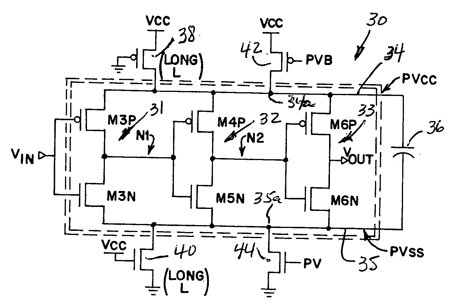
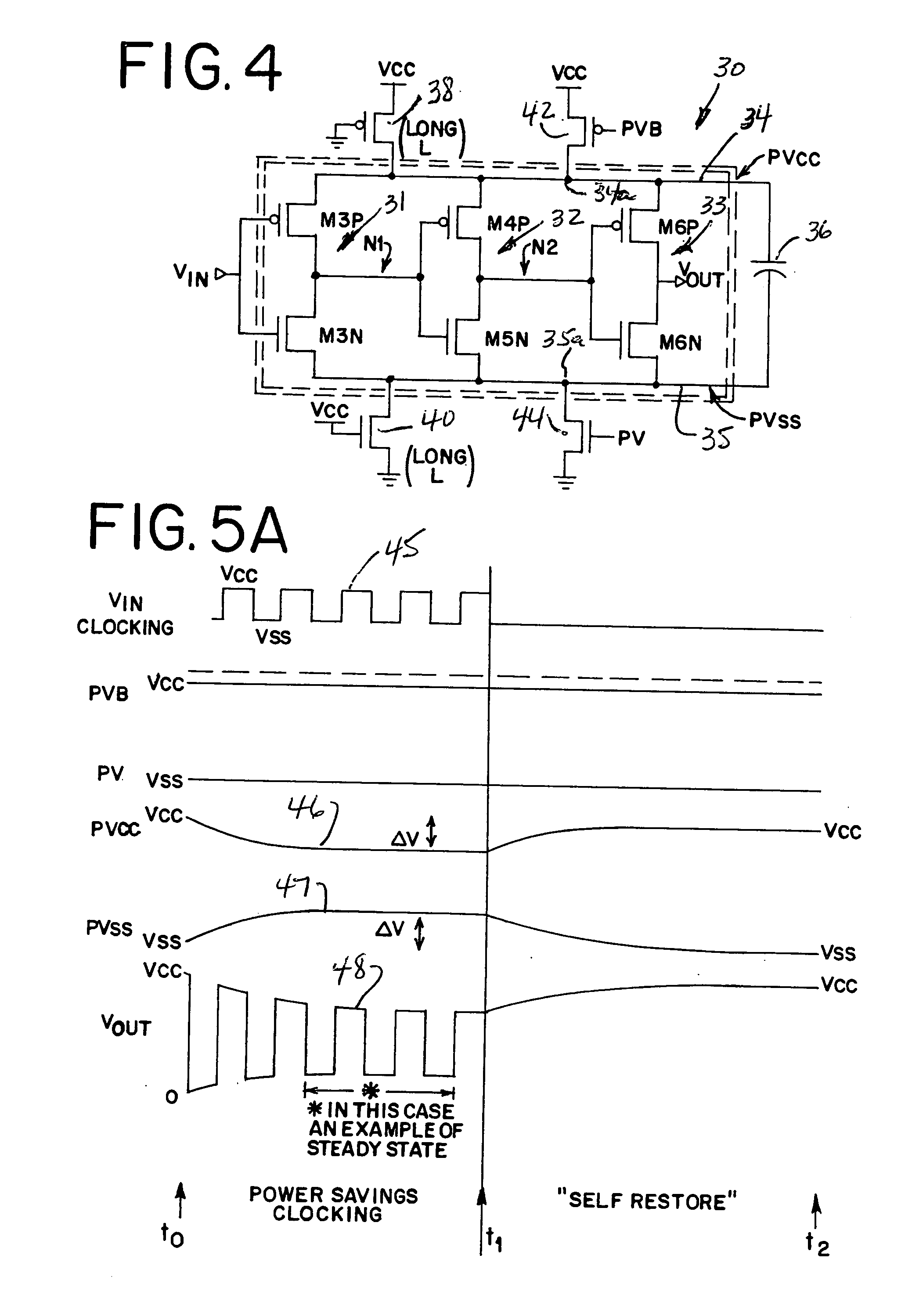
[0058]FIG. 14 illustrates the present invention as applied to a memory circuit, generally designated 110, of the type shown in FIG. 13. In FIG. 14, a capacitor 111 is now disposed between the pseudo power supplies PVcc and PVss on pseudo power supply rails 112 and 113, respectively, with a transistor 114 disposed between positive voltage supply Vss and positive pseudo supply PVss and a transistor 115 disposed between PVss and Vss or ground. Transistors 114 and 115 may have long channel lengths as previously described with respect to FIG. 4 or may comprise other types of biased transistors, resistors or the like. Thus, because of the impedances 114-115 disposed between Vcc and PVcc and between PVss and Vss, respectively, pseudo power supplies PVcc and PVss now become the actual power lines used by most or all of the memory circuit 116 except for the output buffer QBUF 117, and capacitor 111 now supplies the switching or crowbar currents during switching of most of the memory circuit ...
second embodiment
[0060]FIG. 15 illustrates the present invention with respect to a memory circuit, generally designated 120. In this embodiment, output buffer QBUF 127 also operates between pseudo voltage supplies PVcc and PVss on pseudo voltage supply rails 122 and 123, respectively, and a capacitor 121. Thus, unlike memory circuit 110 of FIG. 14, the output buffer 127 of FIG. 15 also takes advantage of crowbar current power savings during switching. This is possible because the outputs Qout and Qoutb on output lines 128 and 129 of the output buffer 127 are differential. That is, when Qout is at a high level, Qoutb is at a low level. Such differential signals do not require full CMOS switching levels, as between supply voltages Vcc and Vss, in order to properly interface with additional circuitry. Only one of the signals Qout or Qoutb needs to be higher than the other signal. Such an interface for the output of buffer 127 requires that the next circuit also has the capability to handle differential...
PUM
 Abstract
Description
Claims
Application Information
 - R&D
- Intellectual Property
- Life Sciences
- Materials
- Tech Scout
- Unparalleled Data Quality
- Higher Quality Content
- 60% Fewer Hallucinations
Browse by: Latest US Patents, China's latest patents, Technical Efficacy Thesaurus, Application Domain, Technology Topic, Popular Technical Reports.
© 2025 PatSnap. All rights reserved.Legal|Privacy policy|Modern Slavery Act Transparency Statement|Sitemap|About US| Contact US: help@patsnap.com


