Oscillator
a technology of oscillator and oscillator, which is applied in the field of oscillators, can solve the problems of large circuit size, low precision of oscillator, and inability to have symmetry in circuit configuration, and achieve the effect of simple configuration and high precision
- Summary
- Abstract
- Description
- Claims
- Application Information
AI Technical Summary
Benefits of technology
Problems solved by technology
Method used
Image
Examples
first embodiment
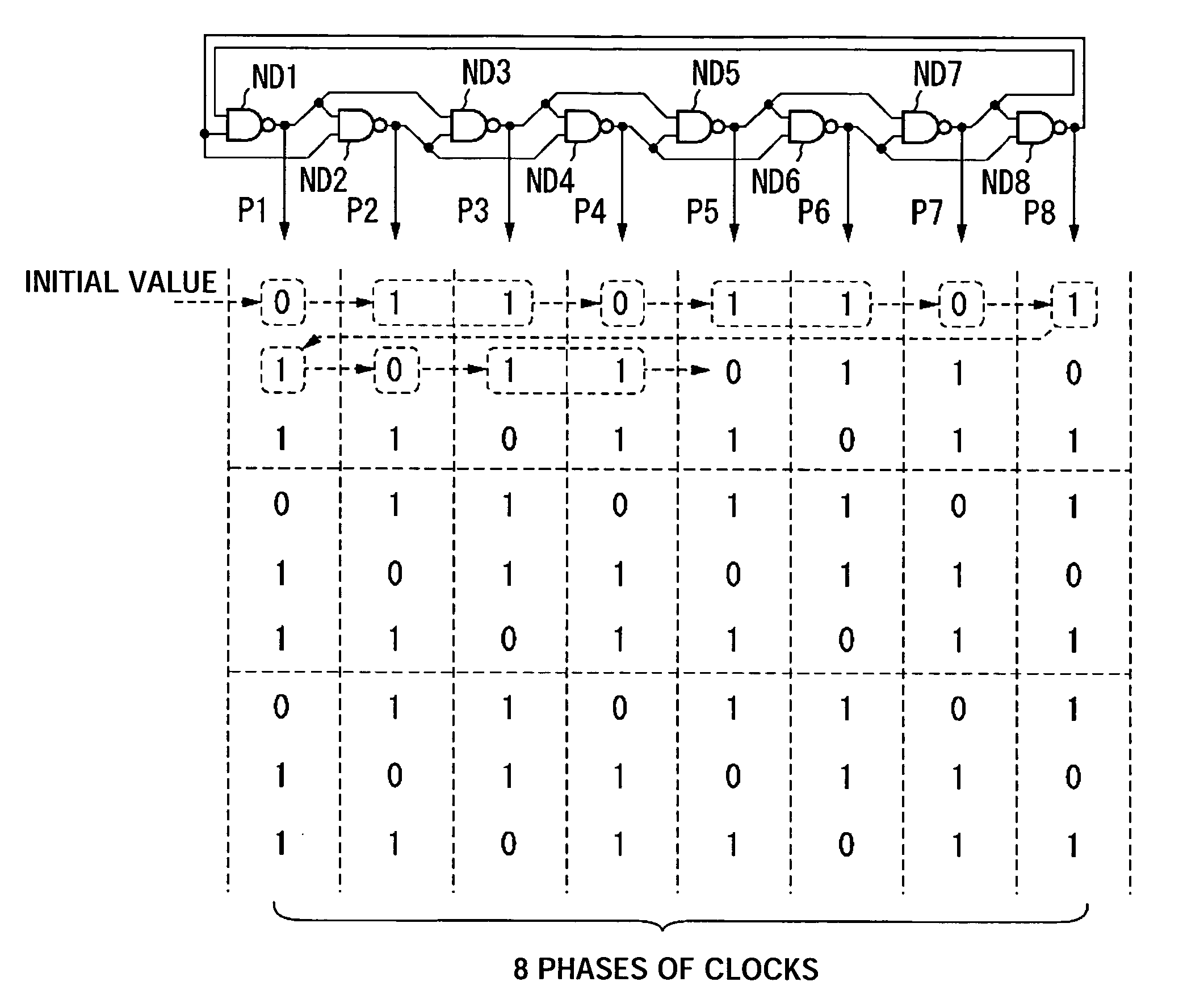
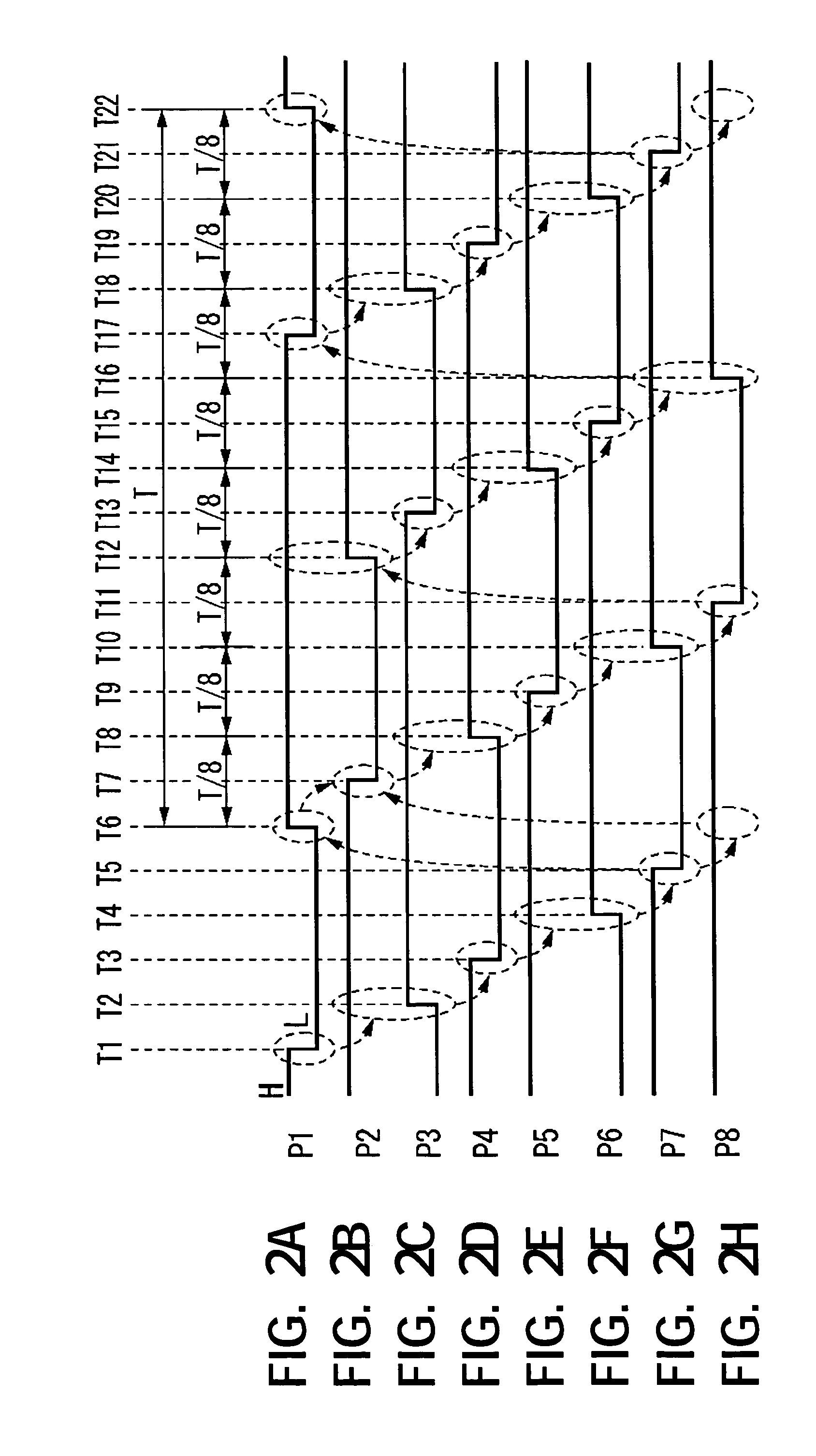
[0037]FIG. 1 is a view for explaining the configuration of an oscillator according to a first embodiment of the present invention and the operation thereof. As shown in FIG. 1, the oscillator according to the first embodiment is formed by eight NAND circuits ND1 to ND8 sequentially connected in a ring. Clock signals P1 to P8 are output from the output nodes of the NAND circuits ND1 to ND8.
[0038] Here, in the oscillator shown in FIG. 1, eight NAND circuits each having two input terminals are connected in a ring. The output node of each of the NAND circuits ND1 to ND8 is connected to one input node of each of the NAND circuits up to the NAND circuit exactly the number of input terminals' worth of places, that is, two places, ahead.
[0039] Namely, for example, the output node of the NAND circuit ND1 is connected to one input node of the NAND circuit ND2 connected one place ahead and one input node of the NAND circuit ND3 connected two places ahead. In the same way, the output node of ...
second embodiment
[0062]FIG. 4 is a view for explaining the configuration of an oscillator according to a second embodiment of the present invention and the operation thereof. As shown in FIG. 4, the oscillator according to the second embodiment is formed by six NAND circuits ND11 to ND16 sequentially connected in a ring. Clock signals P1 to P6 are output from the output nodes of the NAND circuits ND11 to ND16.
[0063] Here, in the oscillator shown in FIG. 4, six NAND circuits each having three input terminals are connected in a ring. The output node of each of the NAND circuits ND11 to ND16 is connected to the input node of each of the NAND circuits up to the NAND circuit exactly the number of input terminals' worth of places, that is, three places, ahead.
[0064] Namely, for example, the output node of the NAND circuit ND11 is connected to one input node of the NAND circuit ND12 connected one place ahead, one input node of the NAND circuit ND13 connected two places ahead, and one NAND circuit ND14 co...
third embodiment
[0080]FIG. 6 is a view for explaining the configuration of an oscillator according to a third embodiment of the present invention and the operation thereof. As shown in FIG. 6, the oscillator according to the third embodiment is formed by six NAND circuits ND21 to ND26 sequentially connected in a ring. Clock signals P1 to P6 are output from the output nodes of the NAND circuits ND21 to ND26.
[0081] Here, in the oscillator shown in FIG. 6, six NAND circuits each having four input terminals are connected in a ring. The output node of each of the NAND circuits ND21 to ND26 is connected to the input node of each of the NAND circuits up to the NAND circuit exactly the number of input terminals' worth of places, that is, four places, ahead.
[0082] Namely, for example, the output node of the NAND circuit ND21 is connected to one input node of the NAND circuit ND22 connected one place ahead, one input node of the NAND circuit ND23 connected two places ahead, the NAND circuit ND24 connected ...
PUM
 Abstract
Description
Claims
Application Information
 - R&D
- Intellectual Property
- Life Sciences
- Materials
- Tech Scout
- Unparalleled Data Quality
- Higher Quality Content
- 60% Fewer Hallucinations
Browse by: Latest US Patents, China's latest patents, Technical Efficacy Thesaurus, Application Domain, Technology Topic, Popular Technical Reports.
© 2025 PatSnap. All rights reserved.Legal|Privacy policy|Modern Slavery Act Transparency Statement|Sitemap|About US| Contact US: help@patsnap.com


