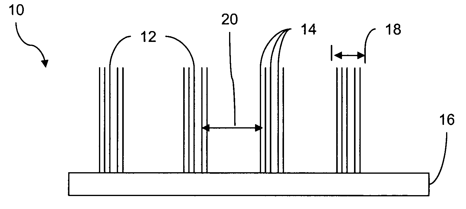
Carbon nanotube high-current-density field emitters
a carbon nanotube and high-current density technology, applied in the manufacture of discharge tube main electrodes, discharge tube/lamp manufacture, electrode systems, etc., can solve the problems of repeatability and emission longevity, no agreement on the optimum geometry, and high emission capability of a single nanotube that does not necessarily transla
- Summary
- Abstract
- Description
- Claims
- Application Information
AI Technical Summary
Benefits of technology
Problems solved by technology
Method used
Image

Examples
examples
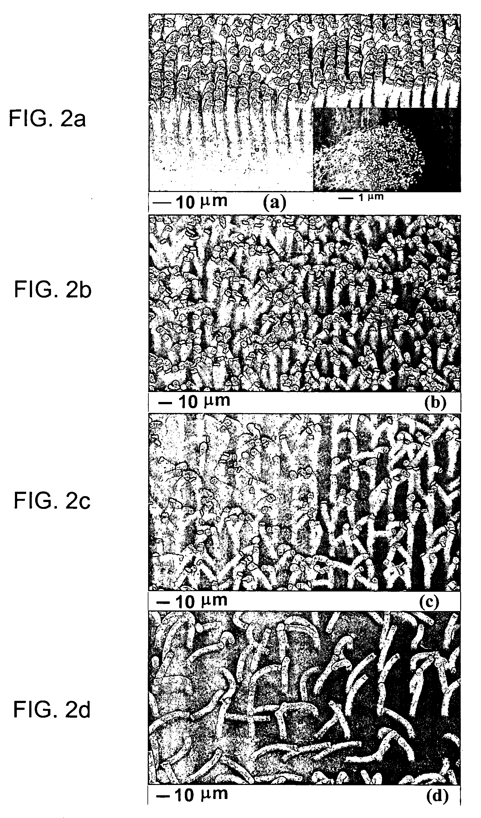
[0027] The scope of the invention will also be understood with reference to the following, non-limiting examples, which are provided to show the optimum geometry for field emitters in accordance with the current invention.
[0028] A variety of field emission tests were performed to find the optimal architecture range for the bundle array field emitters of the current invention. It should be understood that these tests and the emitters are only exemplary embodiments and any emitters formed in accordance with the current invention may be used. A schematic diagram of one of the exemplary bundle array patterns that was used for field emission testing is shown in FIG. 4. As shown, dots of catalyst for growing bundles with diameters of 5 μm, 2 μm, 1 μm, 0.5 μm and 0.2 μm were written by lithography in arrays of size 0.5 mm×20 mm. Six such arrays were written for each dot size, with six different edge-to-edge spacing between dots: 100 μm, 50 μm, 20 μm, 10 μm, 5 μm and 2 μm. By scanning a pr...
PUM
| Property | Measurement | Unit |
|---|---|---|
| diameter | aaaaa | aaaaa |
| length | aaaaa | aaaaa |
| electric field | aaaaa | aaaaa |
Abstract
Description
Claims
Application Information
 - R&D
- Intellectual Property
- Life Sciences
- Materials
- Tech Scout
- Unparalleled Data Quality
- Higher Quality Content
- 60% Fewer Hallucinations
Browse by: Latest US Patents, China's latest patents, Technical Efficacy Thesaurus, Application Domain, Technology Topic, Popular Technical Reports.
© 2025 PatSnap. All rights reserved.Legal|Privacy policy|Modern Slavery Act Transparency Statement|Sitemap|About US| Contact US: help@patsnap.com