Microprocessor architecture capable of supporting multiple heterogeneous processors

a microprocessor and processor technology, applied in the direction of multi-programming arrangements, memory adressing/allocation/relocation, instruments, etc., can solve the problem of maintaining the priority of row match, and achieve the effect of reducing memory latency, reducing wires needed, and adding more latency to memory requests

Inactive Publication Date: 2006-03-23
SAMSUNG ELECTRONICS CO LTD
View PDF35 Cites 23 Cited by
  • Summary
  • Abstract
  • Description
  • Claims
  • Application Information

AI Technical Summary

Benefits of technology

[0017] In practice, other request attributes such as, for example, a function code and a data width attribute are not sent on the SW_REQ because of timing constraints. If the information were to be carried over the switch, it would arrive at the port one phase later than needed, adding more latency to memory requests. Therefore, such request attributes are sent to the port on dedicated wires so that the port can start its state machine earlier and thereby decrease memory latency.
[0018] Referring to FIG. 8, the bus SW_WD comprises 32 wires and is used to send the write data from the master device (D-cache and IOU) to the FIFO at the memory port. It should be noted that the I-cache reads data only and does not write data. This tri-state bus is “double-pumped” which means that a word of data is transferred on each clock phase, reducing the wires needed, and thus the circuit costs. WD00, W01, WD10 and WD11 are words of data. Since the buses are double-pumped, care is taken to insure that there is no bus conflict when the buses turn around and switch from a master to a new master.
[0026] The test and set bypass circuit implements a simple algorithm that prevents a loss of memory bandwidth due to spin-locking, i.e. repeated requests for access to the MAU system bus, for a semaphore. When a test instruction is executed on a semaphore which locks a region of memory, device or the like, the CAM stores the address of the semaphore. This entry in the CAM is cleared when any processor performs a write to a small region of memory enclosing the semphore. If the requested semaphore is still resident in the CAM, the semaphore has not been released by another processor and therefore there is no need to actually access memory for the semaphore. Instead, a block of logical 1's ($FFFF's) (semaphore failed) is sent back to the requesting cache indicating that the semaphore is still locked and the semaphore is not actually accessed, thus saving memory bandwidth.
[0028] The function of the row match comparison circuit is to determine if the present request has the same row address as the previous request. If it does, the port need not de-assert RAS and incur a RAS pre-charge time penalty. Thus, memory latency can be reduced and usable bandwidth increased. Row match is mainly used for dynamic random access memory (DRAM) but it can also be used for static random access memory (SRAM) or read-only memory (ROM) in that the MAU now need not latch in the upper bits of a new address. Thus, when there is a request for access to the memory, the address is sent on the switch network address bus SW_REQ, the row address is decoded and stored in a MUX latch. If this address is considered the row address of a previous request, when a cache or an IOU issues a new request, the address associated with the new address is decoded and its row address is compared with the previous row address. If there is a match, a row match hit occurs and the matching request is given priority as explained below.

Problems solved by technology

There is a limit whereby row match priority can be maintained, however.

Method used


Image

  • Microprocessor architecture capable of supporting multiple heterogeneous processors
  • Microprocessor architecture capable of supporting multiple heterogeneous processors
  • Microprocessor architecture capable of supporting multiple heterogeneous processors

Examples


Embodiment Construction

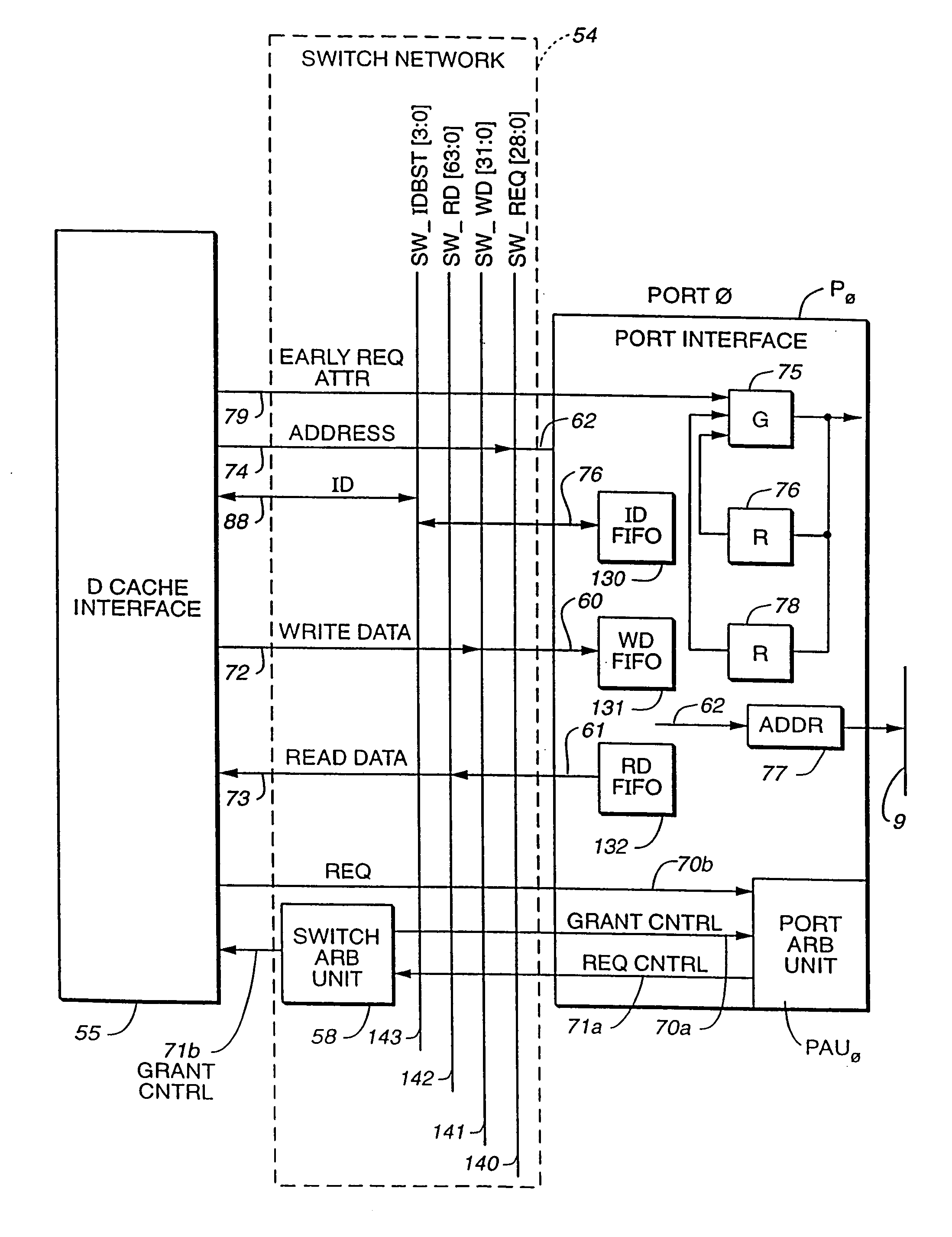
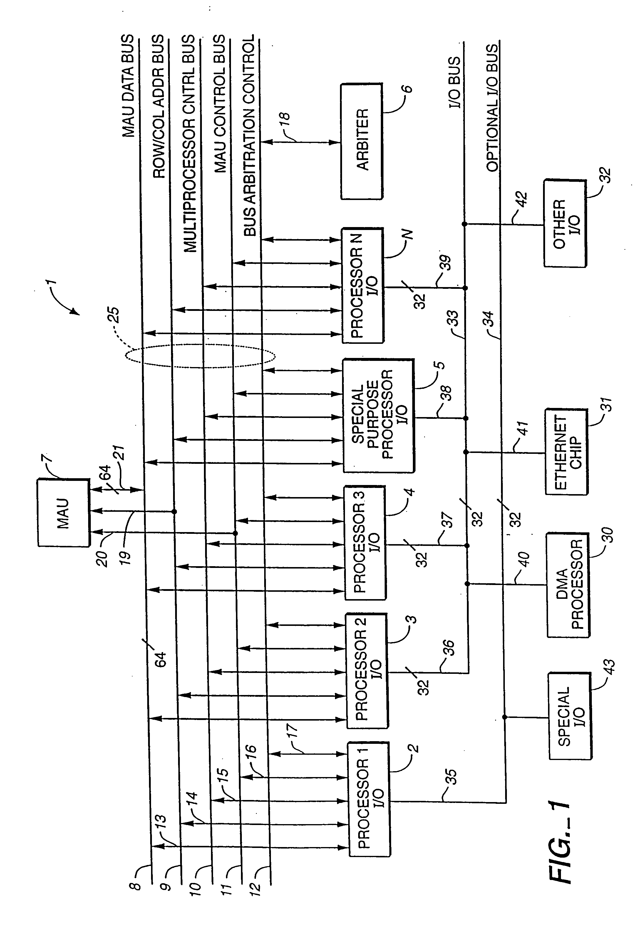
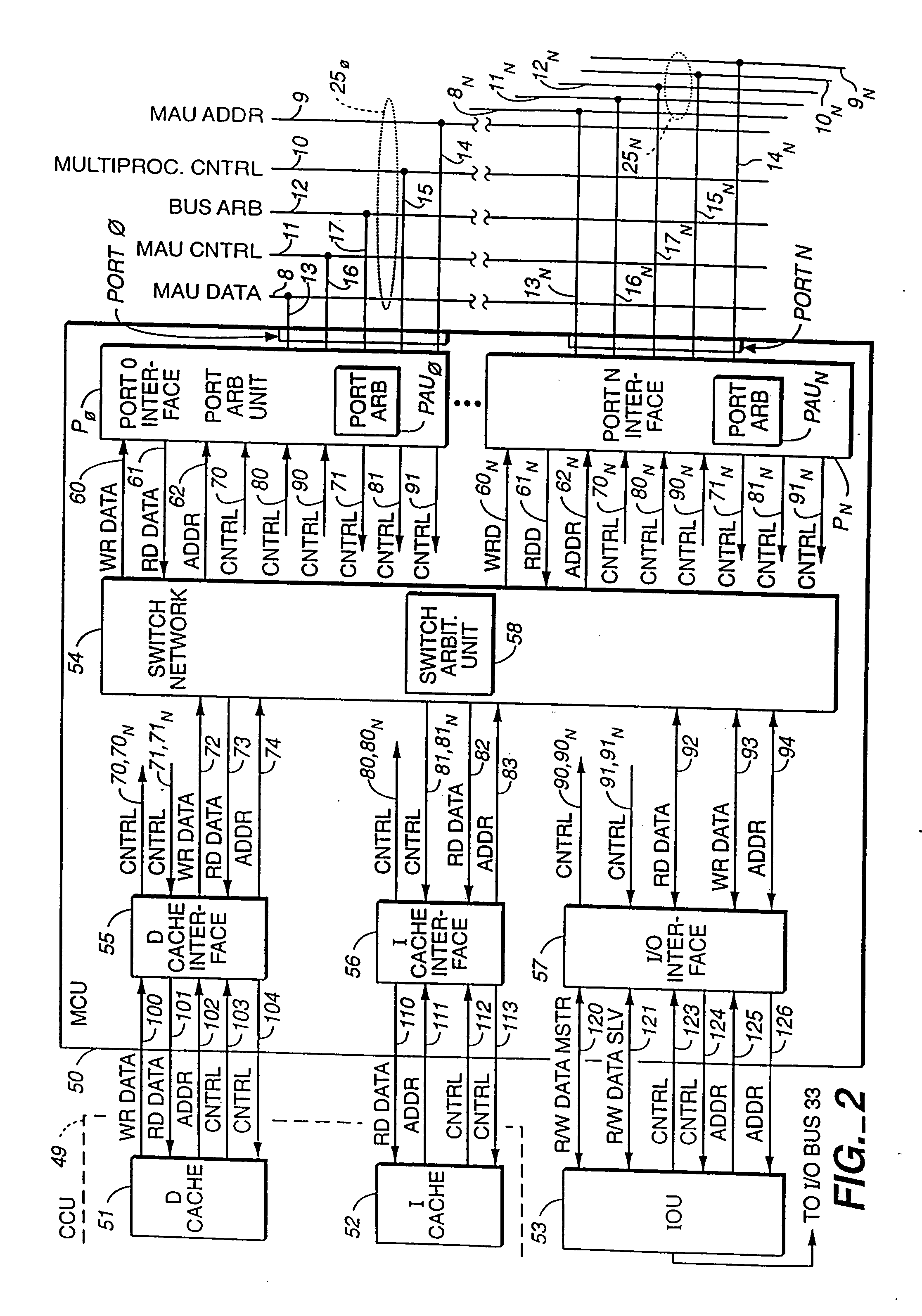
[0052] Referring to FIG. 1, there is provided in accordance with the present invention a microprocessor architecture designated generally as 1. In the architecture 1 there is provided a plurality of general purpose microprocesors 2, 3, 4 . . . N, a special purpose processor 5, an arbiter 6 and a memory / memory array unit (MAU) 7. The microprocessors 2-N may comprise a plurality of identical processors or a plurality of heterogeneous processors. The special purpose processor 5 may comprise, for example, a graphics controller. All of the processors 2-5 are coupled via one or more memory ports PORTD . . . PORTN to an MAU system bus 25 comprising an MAU data bus 8, a ROW / COL address bus 9, a multiprocessor control bus 10, an MAU control bus 11 and a bus arbitration control signal bus 12 by means of a plurality of bidirectional signal buses 13-17, respectively. The bus 12 is used, for example, for requesting arbitration to access and for granting or indicating that the system data bus 8 i...


PUM


Abstract

A memory control unit for controlling access, by one or more devices within a processor, to a memory array unit external to the processor via one or more memory ports of the processor. The memory control unit includes a switch network to transfer data between the one or more devices of the processor and the one or more memory ports of the processor. The memory control unit also includes a switch arbitration unit to arbitrate for the switch network, and a port arbitration unit to arbitrate for the one or more memory ports.

Description

CROSS REFERENCE TO RELATED APPLICATIONS [0001] The present application is a continuation of application Ser. No. 10 / 449,018, filed Jun. 2, 2003, now allowed, which is a continuation of application Ser. No. 09 / 884,943, filed Jun. 21, 2001, now U.S. Pat. No. 6,611,908, which is a continuation of application Ser. No. 09 / 253,761, filed Feb. 22, 1999, now U.S. Pat. No. 6,272,579, which is a divisional application of application Ser. No. 08 / 915,913, filed Aug. 21, 1997, now U.S. Pat. No. 5,941,979, which is a continuation application of application Ser. No. 08 / 442,649 filed May 16, 1995, now U.S. Pat. No. 5,754,800, which is a divisional application of application Ser. No. 07 / 726,893 filed Jul. 8, 1991, now U.S. Pat. No. 5,440,752. The present application is also related to the following applications: [0002] 1. HIGH-PERFORMANCE RISC MICROPROCESSOR ARCHITECTURE, invented by Le Nguyen et al, SMOS-7984MCF / GBR, application Ser. No. 07 / 727,066, filed Jul. 8, 1991, now abandoned; [0003] 2. EXTE...

Claims


Application Information

Patent Timeline
Patent Type & Authority Applications(United States)
IPC IPC(8): G06F15/76G06F9/46G06F9/52G06F12/00G06F12/02G06F12/06G06F12/08G06F13/18G06F13/362G06F13/40G06F15/167G06F15/17G06F15/173G06F15/177
CPCG06F12/0215G06F12/0813G06F12/0831G06F12/0855G06F15/173G06F13/4022G06F15/167G06F15/17G06F13/18G06F15/16
Inventor LENTZ, DEREK J.HAGIWARA, YASUAKILAU, TE-LITANG, CHENG-LONGNGUYEN, LE TRONG
Owner SAMSUNG ELECTRONICS CO LTD
Why Eureka
Try Eureka