
Charge pump circuit

a charge pump and circuit technology, applied in the direction of pulse technique, process and machine control, instruments, etc., can solve the problems of inability to meet the requirements of the conventional charge pump circuit, and the effect of affecting the efficiency of the charge pump circui

Active Publication Date: 2006-03-23
EMEMORY TECH INC
View PDF13 Cites 17 Cited by
  • Summary
  • Abstract
  • Description
  • Claims
  • Application Information

AI Technical Summary

Benefits of technology

[0012] The main objective of the present invention is to provide a charge pump circuit that prevents the occurrence of the body effect, whereby the efficiency of the circuit is enhanced. To accomplish the objective, the charge pump circuit comprises:

Problems solved by technology

However, some deficiencies of the conventional charge pump circuits still exist.
Therefore, when a charge pump circuit utilizes the N-channel type MOSFETs as the main pass transistors, the N-channel type MOSFETs can not be quickly activated thus causing an undesired delay result in the flowing of the charge current through the boosting stages.
The efficiency of the charge pump circuit will accordingly be negatively influenced.

Method used


Image

  • Charge pump circuit
  • Charge pump circuit
  • Charge pump circuit

Examples


Embodiment Construction

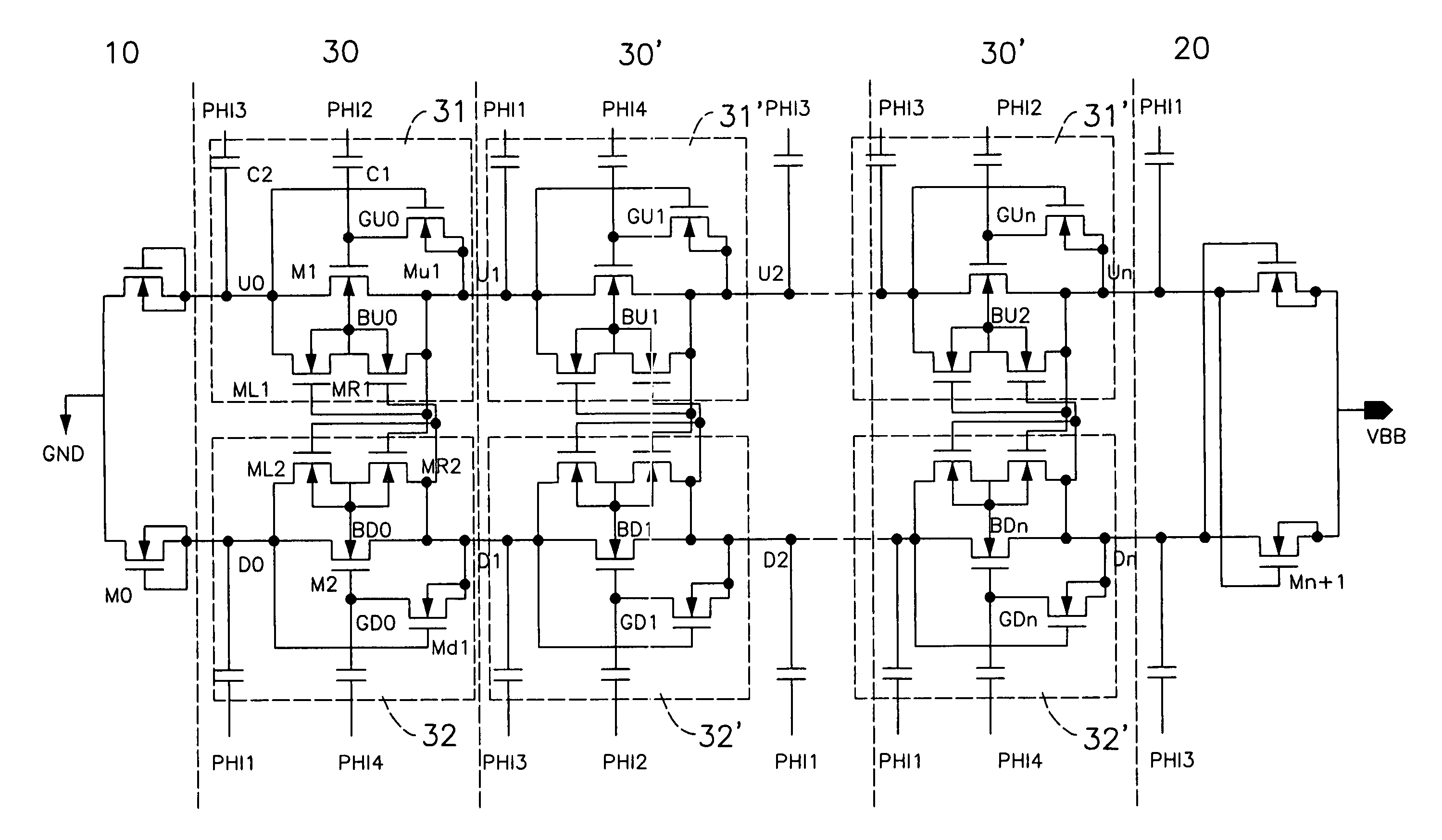
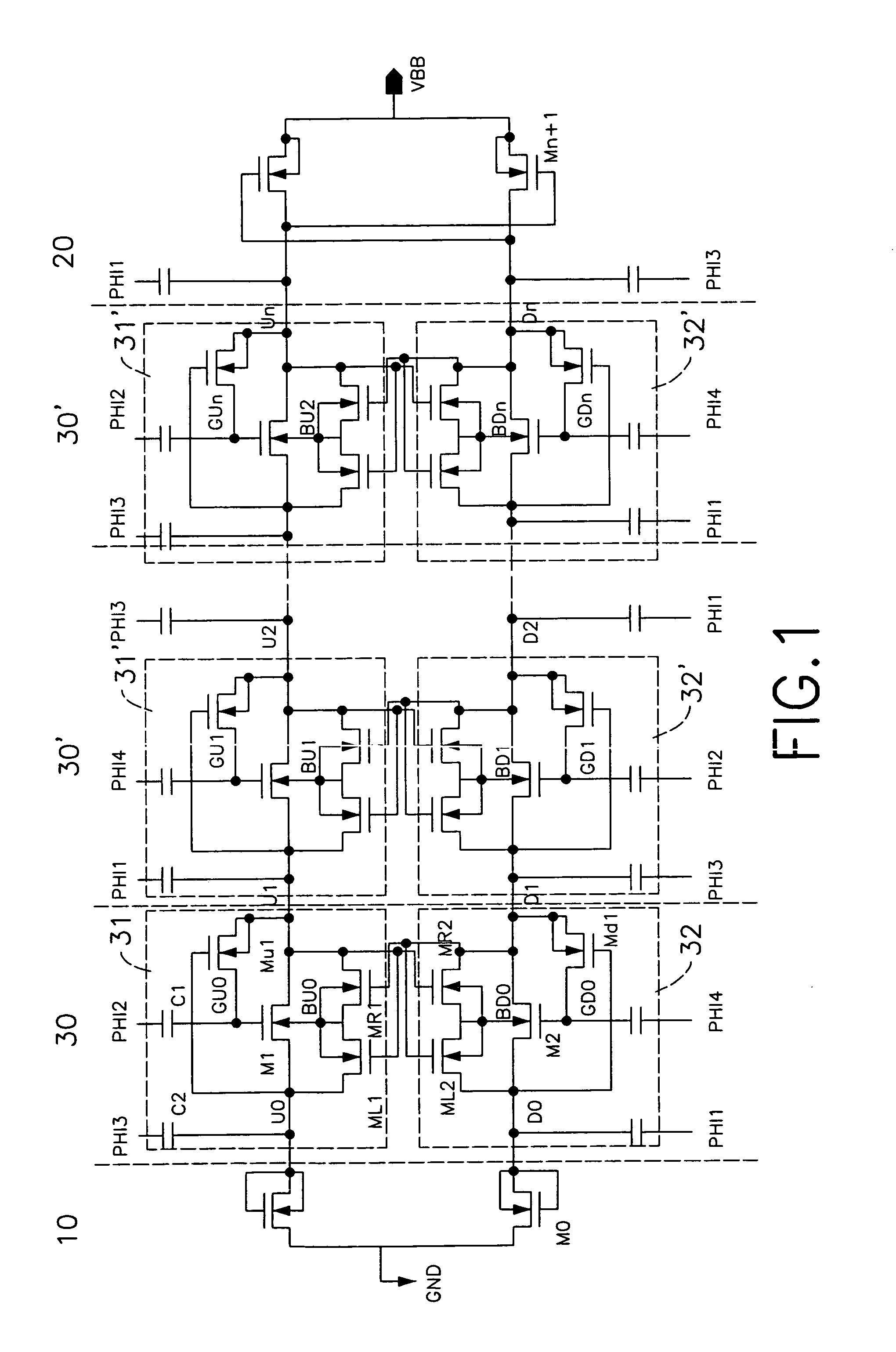
[0024] With reference to FIG. 1, a negative voltage charge pump circuit in accordance with the present invention comprises an input stage (10), an output stage (20), and multiple boosting stages (30)(30′) coupled between the input stage (10) and the output stage (20).

[0025] Each boosting stage (30)(30′) has an upper branch charge pump (31)(31′) and a lower branch charge pump (32)(32′). Using the first boosting stage (30) as an example, the upper branch charge pump (31) comprises a main pass transistor M1, a pre-charge transistor Mu1, two capacitors C1, C2 and two substrate transistors ML1, MR1.

[0026] The main pass transistor M1 has a body, a gate terminal, a source terminal and a drain terminal. The source terminal and the drain terminal are respectively used as a first node U0 and a second node U1, and are respectively coupled to a front stage (the input stage (10) in the example) and a rear stage (the second boosting stage (30′)). The pre-charge transistor Mul provides its sourc...


PUM


Abstract

A charge pump circuit has an input stage, an output stage and multiple boosting stages coupled between the input stage and the output stage. The boosting stages are driven by four phase clock signals. Each boosting stage has two branch charge pumps, wherein each branch charge pump at least has a main pass transistor, a pre-charge transistor, two substrate transistors and capacitors. The substrate transistors and the main pass transistor are operated in association with the four phase clock signals to keep a potential of the body of the main pass transistors at a low level thus mitigating the body effect.

Description

BACKGROUND OF THE INVENTION [0001] 1. Field of the Invention [0002] The present invention relates to a charge pump circuit, and more particularly to a charge pump circuit that effectively prevents an occurrence of a body effect of metal oxide semiconductor field-effect transistors (MOSFETs). [0003] 2. Description of Related Art [0004] In order to lower power consumption, an operating voltage for integrated circuits (ICs) is modified to a lower level. For example, the normal operating voltage for the ICs has been changed from the early 5 volts to the present 3.3 volts, and sometimes even lower than 2 volts. Although a lower operating voltage is beneficial for power consumption reduction, some particular applications requiring a high operating voltage still should be concerned. In particular, while erasing data stored in a flash memory, a large negative voltage, usually −9 or −10 volts, is necessary and supplied by a charge pump circuit. [0005] A conventional negative voltage charge p...

Claims


Application Information

Patent Timeline
IPC IPC(8): G05F1/10
CPCH02M3/073H03K2217/0018H02M2003/075H02M3/075
Inventor CHIU, LIANG-HSIANGCHANG, WU-CHANG
Owner EMEMORY TECH INC
Learn More