Memory controller transaction scheduling algorithm using variable and uniform latency

a transaction scheduling and memory controller technology, applied in the direction of instruments, computing, electric digital data processing, etc., can solve the problems of large variation in signal propagation duration between memory controller and device, low efficiency of memory channel at high utilization, and variable latency to multiple memory devices

Inactive Publication Date: 2006-02-02
INTEL CORP
View PDF6 Cites 40 Cited by
  • Summary
  • Abstract
  • Description
  • Claims
  • Application Information

AI Technical Summary

Problems solved by technology

Likewise, certain topologies, for example a point-to-point memory topology, may have additional delays at each point (node), causing greater variation in signal propagation duration between the memory controller and the devices.
Unfortunately, latency to multiple memory devices can vary.
Unfortunately, if a memory controller has variable latency then the efficiency of the memory channel may drop at high utilizations, for example, from scheduling conflicts (bubbles) due to the variable read latency feature.

Method used


Image

  • Memory controller transaction scheduling algorithm using variable and uniform latency
  • Memory controller transaction scheduling algorithm using variable and uniform latency
  • Memory controller transaction scheduling algorithm using variable and uniform latency

Examples


Embodiment Construction

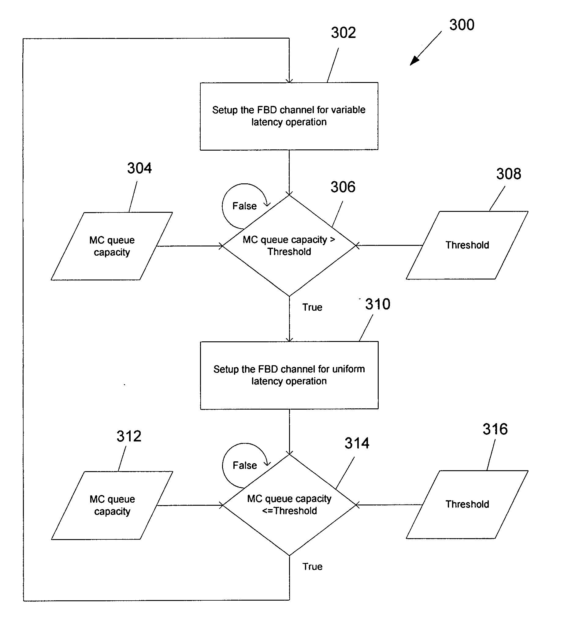
[0008] Inventive principles illustrated in this disclosure are not limited to the specific details disclosed herein.

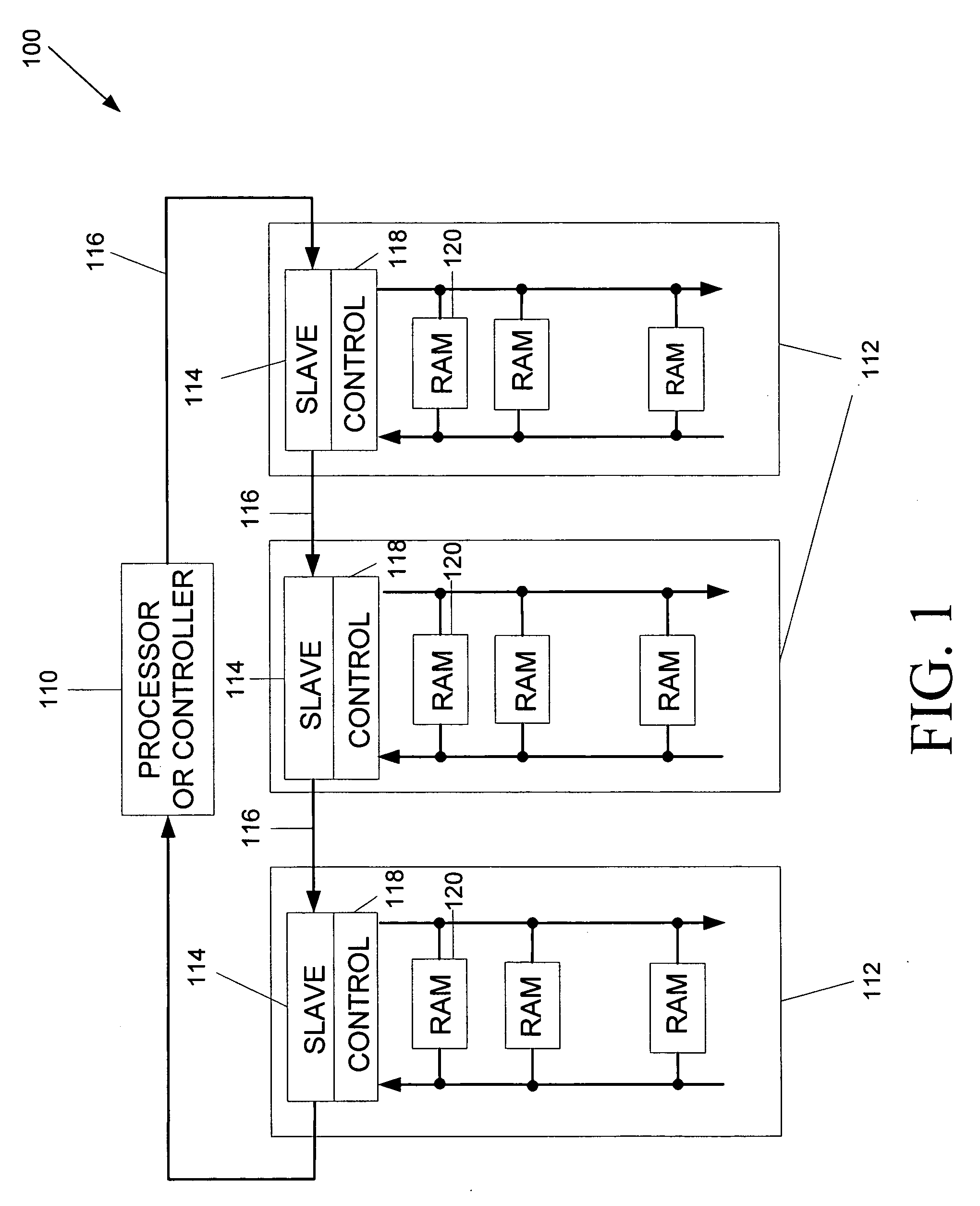
[0009] A review of a conventional memory architecture will aid understanding of methods of the present invention. FIG. 1 illustrates a prior art memory system known informally as RamLink, which was proposed as a standard by the Institute of Electrical and Electronics Engineers (IEEE). The standard was designated as IEEE Std 1596.4-1996 and is known formally as IEEE Standard for High-Bandwidth Memory Interface Based on Scalable Coherent Interface (SCI) Signaling Technology (RamLink).

[0010] The system of FIG. 1 includes a processor or controller 110 (memory controller) and one or more memory modules 112. The memory controller 110 is typically either built into a processor or fabricated on a companion chipset for a processor, but may be any logic device that can operate with the memory channel. Each memory module 112 has a slave interface 114 that has one link input and...


PUM


Abstract

A memory method may select a latency mode, such as read latency mode, based on measuring memory channel utilization. Memory channel utilization, for example, may include measurements in a memory controller queue structure. Other embodiments are described and claimed.

Description

BACKGROUND OF THE INVENTION [0001] Conventional memory controllers often control multiple memory devices including modules, chips, Dual Inline Memory Modules (DIMMs), agents, etc. Distances from the memory controller to controlled devices may vary, resulting in different signal propagation times between the memory controller and the devices. Likewise, certain topologies, for example a point-to-point memory topology, may have additional delays at each point (node), causing greater variation in signal propagation duration between the memory controller and the devices. [0002] Generally, latency is the time between a stimulus and a response to the stimulus. Some conventional memory architectures have uniform latency on a memory channel between a memory controller and its controlled devices. The memory channel may include data paths leading to memory for either control or data signals. Memory channels may also include a memory controller and its controlled devices. In an example uniform ...

Claims


Application Information

Patent Timeline
IPC IPC(8): G06F13/28G06F12/00
CPCG06F13/28
Inventor CHRISTENSON, BRUCE A.NATARAJAN, CHITRA
Owner INTEL CORP
Why Eureka
Try Eureka