Wiring substrate, electronic device, electro-optical device, and electronic apparatus

a technology of wiring substrate and electrooptical device, applied in the field of electrooptical device, can solve the problems of parasitic capacitance generation of electro-optical devices, particularly acute problem caused by capacitance between conductive parts such as wiring lines

Inactive Publication Date: 2006-02-02
BOE TECH GRP CO LTD
View PDF18 Cites 10 Cited by
  • Summary
  • Abstract
  • Description
  • Claims
  • Application Information

AI Technical Summary

Benefits of technology

[0008] The present invention addresses or solves the above and / or other problems, and provides a wiring substrate that can produce stable performance, an electric-optical device that can be used in a large screen display and that can operate stably over a long period of times, and an electronic apparatus using the same.
[0035] Since substances can easily pass through the component, when at least part of the components is covered with the protective film, dispersion of substances via the components can be avoided. Moreover, deterioration or corrosion of the wiring lines or the active elements in the demo-optical device can be reduced. Generally, since a low-dielectric-constant material is mechanically fragile, advantageously, the protective film can mechanically reinforce the components.

Problems solved by technology

Related art electro-optical devices suffer from parasitic capacitance generated between wiring lines and the like during data-overwriting operation or the like.
This has posed a problem in fabricating large screen display devices using electro-optical devices.
Thus the problem caused by the capacitance between conductive parts such as wiring lines is particularly acute.

Method used


Image

  • Wiring substrate, electronic device, electro-optical device, and electronic apparatus
  • Wiring substrate, electronic device, electro-optical device, and electronic apparatus
  • Wiring substrate, electronic device, electro-optical device, and electronic apparatus

Examples


Embodiment Construction

[0058] The present invention is described below in detail.

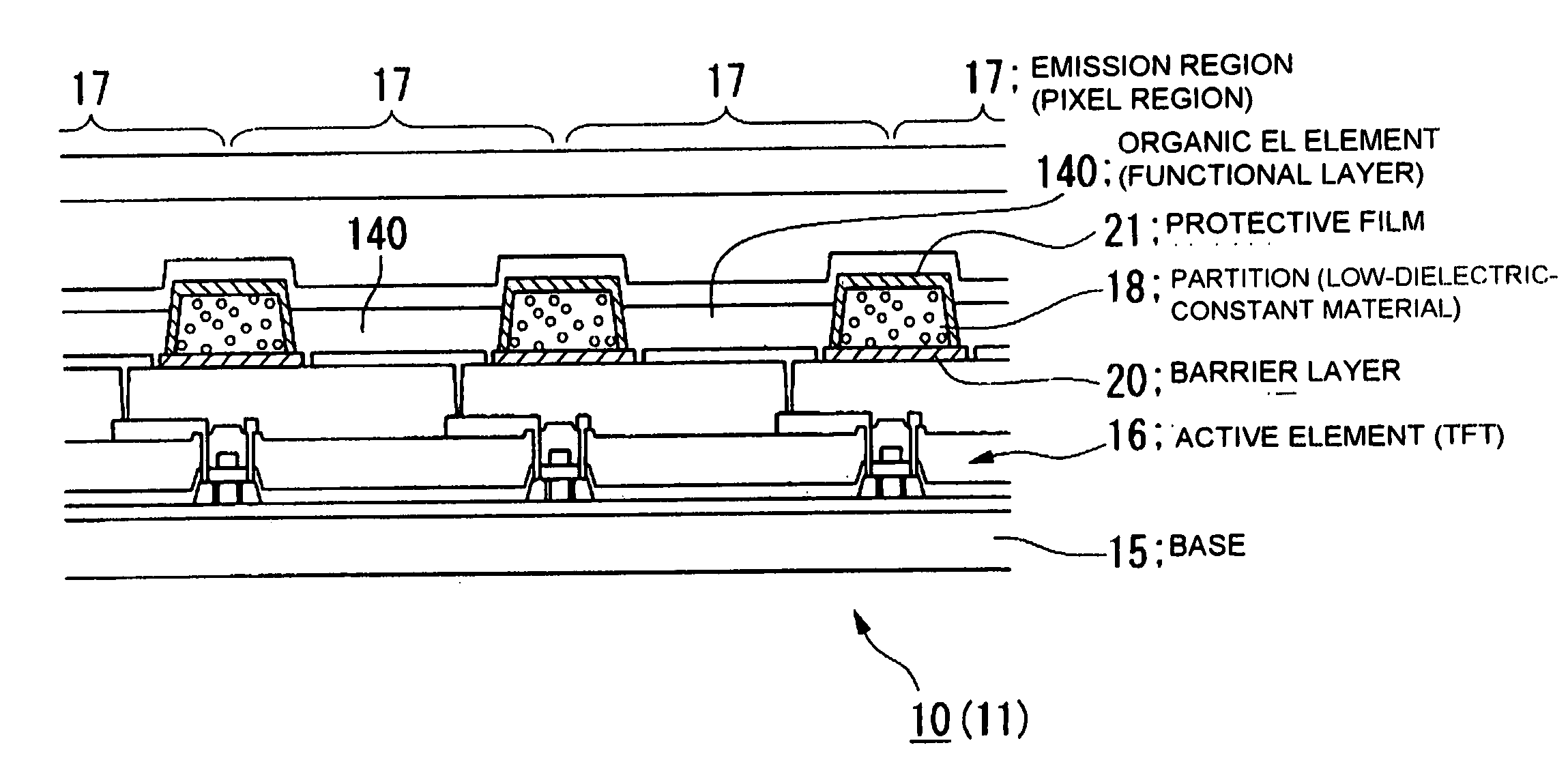
[0059]FIG. 1 is a schematic that conceptually shows the structures of an electro-optical device and a substrate of the present invention in a cross-section. Reference numeral 10 denotes an electro-optical device, and reference numeral 11 denotes a wiring substrate. The wiring substrate 11 is of a multiplayer interconnection type and includes insulating layers and active elements 16, such as thin film transistors (hereinafter “TFTs”), disposed on the base 15. The electro-optical device 10 includes a plurality of light-emitting regions 17 that contain luminescent layers as the functional films and is disposed on the wiring substrate 11. The state of light emission is controlled by using the active elements 16. At borders between the light-emitting regions 17, partitions (banks) 18 functioning as insulating layers are provided.

[0060] The electro-optical device 10 of the present invention is provided such that the partitions 18...


PUM


Abstract

The invention achieves stable performance, such as low parasitic capacitance generated at conductive components. Components having a low dielectric constant of 4 or less are disposed on a base member. Functional films partitioned by the low-dielectric-constant components are also provided.

Description

[0001] This is a Division of application Ser. No. 10 / 383,075 filed Mar. 7, 2003. The entire disclosure of the prior application is hereby incorporated by reference herein in its entirety.BACKGROUND OF THE INVENTION [0002] 1. Field of Invention [0003] The present invention relates to electronic devices, such as electro-optical devices or semiconductor devices, a wiring substrate suitable for use in electronic devices, an electro-optical device suitable for use in display devices, and an electronic apparatus. [0004] 2. Description of Related Art [0005] The related art includes electro-optical devices that are usable as display devices, such as liquid crystal display devices including liquid crystal elements, and organic electroluminescent display devices including organic electroluminescent elements (hereinafter “organic EL elements”). In particular, organic EL display devices have superior display characteristics in that they are highly bright and self-luminous, can be driven by low ...

Claims


Application Information

Patent Timeline
IPC IPC(8): H05K1/16H01L21/77H01L21/84H01L27/12H01L27/32H05K1/02H05K3/46
CPCH01L27/12H01L27/1214H05K2201/0187H05K1/024H05K3/4644H01L27/3246H01L27/1259H10K59/122
Inventor MIYAZAWA, TAKASHI
Owner BOE TECH GRP CO LTD
Why Eureka
Try Eureka