Floating input amplifier for capacitively coupled communication

a capacitively coupled, floating input technology, applied in differential amplifiers, amplifiers with semiconductor devices/discharge tubes, amplifier details, etc., can solve problems such as causing bottlenecks, and affecting the performance of capacitively coupled inter-chip communication

Active Publication Date: 2005-12-29
ORACLE INT CORP
View PDF12 Cites 20 Cited by
  • Summary
  • Abstract
  • Description
  • Claims
  • Application Information

AI Technical Summary

Benefits of technology

[0015] After the input voltage of the input of the amplifier mechanism substantially stabilizes at the switching-threshold voltage of the first stage, the voltage offset correction mechanism is uncoupled from the input. Then, data transmission on the transmitter pad is resumed. In this way, a small input voltage swing on the input is able to trigger an amplified output signal voltage swing.
[0018] In yet another variation on this embodiment, selectively initializing the input voltage of the input of the amplifier mechanism involves setting a bias voltage on one terminal of a capacitor after uncoupling the voltage offset generating mechanism from the input and before resuming data transmission on the transmitter pad. The other terminal of the capacitor is coupled in parallel with the input of the amplifier mechanism. This bias voltage allows fine tuning of the input voltage of the input to the switching-threshold voltage of the first stage of the amplifier mechanism. The bias voltage is selected such that the amplified output signal voltage swing is symmetric between the voltage that represents a logical “1” and the voltage that represents a logical “0”.

Problems solved by technology

Unfortunately, these advances in semiconductor technology have not been matched by corresponding advances in inter-chip communication technology.
This problem is beginning to create a bottleneck that continues to grow as semiconductor integration densities continue to increase.
However, capacitively coupled inter-chip communication poses technical challenges.
This limitation requires a receiver amplifier to set a DC voltage of an input to the receiver amplifier.
It is difficult to set the DC voltage in order to balance signal and noise considerations.
Exacerbating the challenge of setting the DC voltage, the coupling capacitance may vary over two or more orders of magnitude, causing a large variation in signal and noise amplitudes.

Method used


Image

  • Floating input amplifier for capacitively coupled communication
  • Floating input amplifier for capacitively coupled communication
  • Floating input amplifier for capacitively coupled communication

Examples


Embodiment Construction

[0027] The following description is presented to enable any person skilled in the art to make and use the invention, and is provided in the context of a particular application and its requirements. Various modifications to the disclosed embodiments will be readily apparent to those skilled in the art, and the general principles defined herein may be applied to other embodiments and applications without departing from the spirit and scope of the present invention. Thus, the present invention is not intended to be limited to the embodiments shown, but is to be accorded the widest scope consistent with the principles and features disclosed herein.

A Single-Ended Floating-Input Amplifier

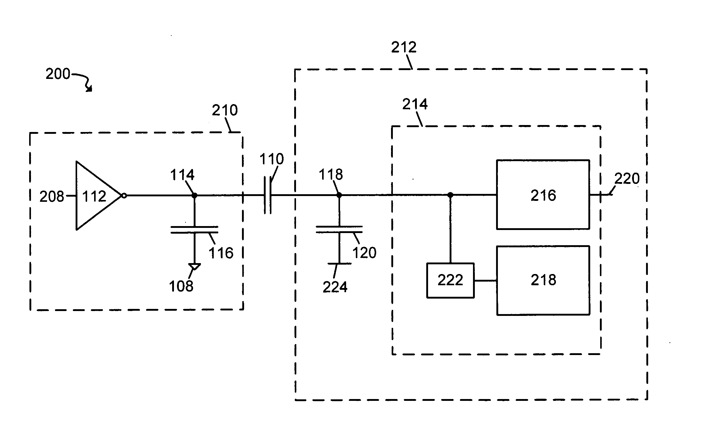
[0028]FIG. 2 illustrates an electric circuit 200 in accordance with an embodiment of the present invention that facilitates capacitive communication of data 208 in the form of electrical signals between a first semiconductor die 210 and a second semiconductor die 212. The inverter 112 in the transmitte...


PUM


Abstract

One embodiment of the present invention provides a capacitively-coupled receiver amplifier that has an input with no DC coupling. A DC voltage is programmed on the input. During programming, a transmitter is held at a voltage at a midpoint between a voltage that represents a logical “1” and a voltage that represents a logical “0” and the input voltage of the receiver amplifier is programmed to be substantially the switching-threshold voltage for the receiver amplifier. Then, during normal data communication, the transmitter drives high and low electrical signals that are coupled to the receiver amplifier. Since the input of the receiver amplifier has been substantially set to the DC voltage, the receiver amplifier need not control the DC voltage of the input for each transition in the electrical signals.

Description

GOVERNMENT LICENSE RIGHTS [0001] This invention was made with United States Government support under Contract No. NBCH020055 awarded by the Defense Advanced Research Projects Administration. The United States Government has certain rights in the invention.BACKGROUND [0002] 1. Field of the Invention [0003] The present invention relates to electronic circuits on semiconductor chips. More specifically, the present invention relates to a capacitively coupled amplifier that facilitates communication between semiconductor chips. [0004] 2. Related Art [0005] Advances in semiconductor technology presently make it possible to integrate large-scale systems, including tens of millions of transistors, into a single semiconductor chip. Integrating such large-scale systems onto a single semiconductor chip increases the speed at which such systems can operate, because signals between system components do not have to cross chip boundaries, and are not subject to lengthy chip-to-chip propagation del...

Claims


Application Information

Patent Timeline
IPC IPC(8): H03F3/08H03F3/45
CPCH03F3/45977H03F3/08
Inventor DROST, ROBERT J.HO, RONALDSUTHERLAND, IVAN E.
Owner ORACLE INT CORP
Why Eureka
Try Eureka