
Current replication to avoid LEB restriction of DC-DC boost converter

Inactive Publication Date: 2005-12-22
INTERSIL INC
View PDF14 Cites 46 Cited by
  • Summary
  • Abstract
  • Description
  • Claims
  • Application Information

AI Technical Summary

Benefits of technology

[0009] A current replication circuit according to an embodiment of the present invention avoids the LEB period restriction of a DC-DC boost converter. The DC-DC boost converter regulates an output voltage by switching an input voltage through an inductor and a diode using a switch controller employing current feedback control and providing a pulse-width modulation (PWM) signal to control a switch coupled to the inductor. The current replication circuit includes a current sensor, a ramp generator, and a summing device. The current sensor samples current through the inductor while the switch is off and provides a sample voltage indicative of inductor current just before the switch is turned on. The ramp generator provides a ramp voltage replicating current increase of the inductor while the switch is on. The summing device adds the sample voltage to the ramp voltage to develop a replication voltage used for feedback current control by the switch controller.
[0014] A method of eliminating the LEB period restriction of a DC-DC boost converter according to an embodiment of the present invention enables reduced PWM duty cycle and an output voltage that is significantly closer to the input voltage than that previously allowed because of the LEB period restriction. The method includes determining current level of the inductor while the switch is open and just before the switch is closed and providing a corresponding current level signal, synthesizing current increase of the inductor while the switch is closed and providing a corresponding ramp signal, and adding the current level and ramp signals together to develop a current feedback sense signal provided to the sample controller.

Problems solved by technology

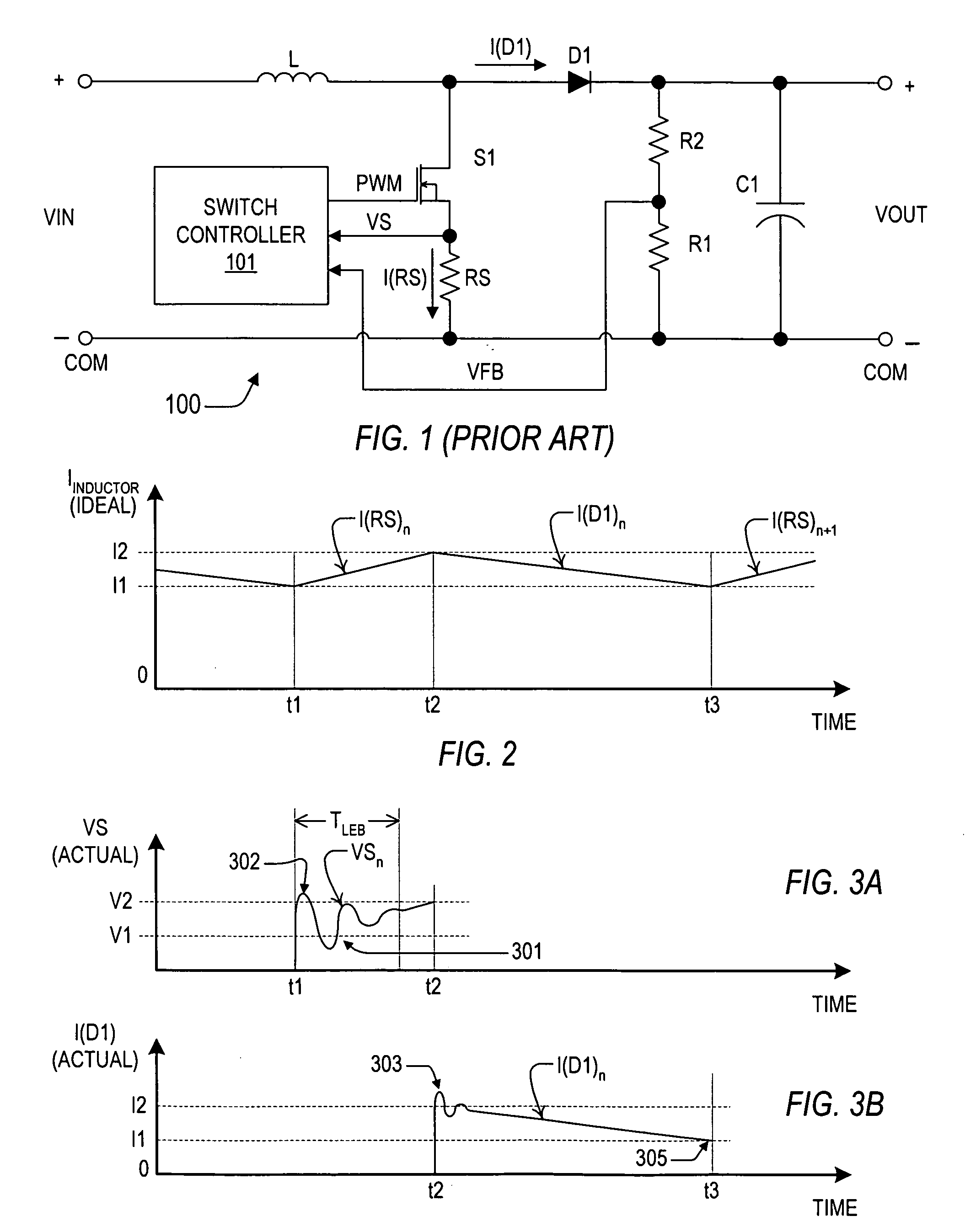
A particular problem with the conventional DC-DC boost converter is the leading-edge ringing that occurs on the inductor current when the switch is turned on (or closed).
The TLEB period, however, restricts the minimum duty cycle of the boost converter and therefore limits the output voltage range for a given input voltage.
Such solution is inherently inefficient in terms of power consumption and the number of components needed.

Method used


Image

  • Current replication to avoid LEB restriction of DC-DC boost converter
  • Current replication to avoid LEB restriction of DC-DC boost converter
  • Current replication to avoid LEB restriction of DC-DC boost converter

Examples


Embodiment Construction

[0025] The following description is presented to enable one of ordinary skill in the art to make and use the present invention as provided within the context of a particular application and its requirements. Various modifications to the preferred embodiment will, however, be apparent to one skilled in the art, and the general principles defined herein may be applied to other embodiments. Therefore, the present invention is not intended to be limited to the particular embodiments shown and described herein, but is to be accorded the widest scope consistent with the principles and novel features herein disclosed.

[0026]FIG. 1 is a simplified schematic diagram of a conventional DC-DC boost converter 100. An input voltage VIN measured with respect to a common node COM (e.g., ground or “power ground”) is applied to one end of an inductor L, having its other end coupled to the drain of a MOSFET switch S1 and to the anode of a diode D1. The switch S1 is shown as a MOSFET, although any othe...


PUM


Abstract

A current replication circuit that avoids the LEB period restriction of a DC-DC boost converter. The DC-DC boost converter regulates an output voltage by switching an input voltage through an inductor and a diode using a switch controller employing current feedback control and providing a PWM signal to control a switch coupled to the inductor. The current replication circuit includes a current sensor, a ramp generator, and a summing device. The current sensor samples current through the inductor while the switch is off and provides a sample voltage indicative of inductor current just before the switch is turned on. The ramp generator provides a ramp voltage replicating current increase of the inductor while the switch is on. The summing device adds the sample voltage to the ramp voltage to develop a replication voltage used for feedback current control by the switch controller.

Description

CROSS-REFERENCE TO RELATED APPLICATIONS [0001] This application claims the benefit of British Patent Application No. 0413494.6, filed on Jun. 16, 2004, which is herein incorporated by reference for all intents and purposes. BACKGROUND OF THE INVENTION [0002] 1. Field of the Invention [0003] The present invention relates to DC-DC converters employing current feedback, and more particularly to a current replication circuit which enables elimination of the leading edge blanking (LEB) period of a DC-DC boost converter to remove the duty cycle restriction. [0004] 2. Description of the Related Art [0005] A conventional DC-DC boost converter switches current through an inductor and diode to convert an input voltage to a larger, regulated output voltage. The switching is typically performed by an electronic switch, such as a metal-oxide semiconductor, field-effect transistor (MOSFET), which has its gate controlled by a pulse-width modulation (PWM) control signal. The drain and source path o...

Claims


Application Information

Patent Timeline
IPC IPC(8): G05F1/40H02M3/158
CPCH02M3/1584
Inventor LEFEVRE, ANDREW P.
Owner INTERSIL INC
Learn More