
Micromirror array assembly with in-array pillars

a micromirror array and array technology, applied in the field of microelectromechanical systems, can solve the problems of inability to ensure uniform distance throughout the array, and inability to achieve desired operation or performance of the device. achieve the effect of enhancing the hermetic seal

Active Publication Date: 2005-12-15
TEXAS INSTR INC +1
View PDF80 Cites 98 Cited by
  • Summary
  • Abstract
  • Description
  • Claims
  • Application Information

AI Technical Summary

Benefits of technology

[0011] In yet another embodiment of the invention, a micromirror array device is disclosed, which comprises: a substrate having thereon an array of micromirrors, further comprising: at least two electrical contact pads, each of which is electrically connected to the micromirrors such that am electrical resistance of the micromirrors of the array can be measured through the electrical contact pads; and an array of electrodes associated with the micromirrors for deflecting t...

Problems solved by technology

These substrates may deform during fabrication or operation, causing degradation of the device performance or even device failure when the deformation exceeds a tolerable amount.
However, a uniform distance throughout the micromirror array may not be guaranteed in fabrication or in operation or in both due to deformation of the substrates on which the micromirrors and electrodes are formed.
As a consequence, desired operation or performance of the device is not achievable.
In addition to the substrate deformation, other factors, such as operation environment (e.g. contamination and viscosity) may also degrade the operation and performance of the micromirror array device.
Viscosity problems arise from the viscosity resistance to the rotation of the mirror plate in a medium, such as air or the gas (e.g. an inert gas).
The viscosity resistance to the movement of the mirror plate reduces the response time of the mirror plate and limits the application of the micromirror array device.

Method used


Image

  • Micromirror array assembly with in-array pillars
  • Micromirror array assembly with in-array pillars
  • Micromirror array assembly with in-array pillars

Examples


Embodiment Construction

[0034] The present invention provides a microstructure device comprising multiple substrates with the functional components of the device formed on the substrates. In order to maintain a uniform gap between the substrates, a plurality of pillars is provided and distributed within the gap. The gap uniformity can further be enhanced by maintaining the pressure inside the gap below the pressure under which the microstructure device will be in operation.

[0035] In the following, the present invention will be discussed with reference to examples in which a microelectromechanical device comprises an array of micromirrors formed on two substrates. It is understood by those skilled in the art that the following discussion is for demonstration purposes only and will not be interpreted as a limitation. Though the invention will be discussed with reference to the following example, it is not intended to exclude other variations within the scope of the present invention. For example, the presen...


PUM


Abstract

The present invention provides a microstructure device comprising multiple substrates with the components of the device formed on the substrates. In order to maintain uniformity of the gap between the substrates, a plurality of pillars is provided and distributed in the gap so as to prevent decrease of the gap size. The increase of the gap size can be prevented by bonding the pillars to the components of the microstructure. Alternatively, the increase of the gap size can be prevented by maintaining the pressure inside the gap below the pressure under which the microstructure will be in operation. Electrical contact of the substrates on which the micromirrors and electrodes are formed can be made through many ways, such as electrical contact areas, electrical contact pads and electrical contact springs.

Description

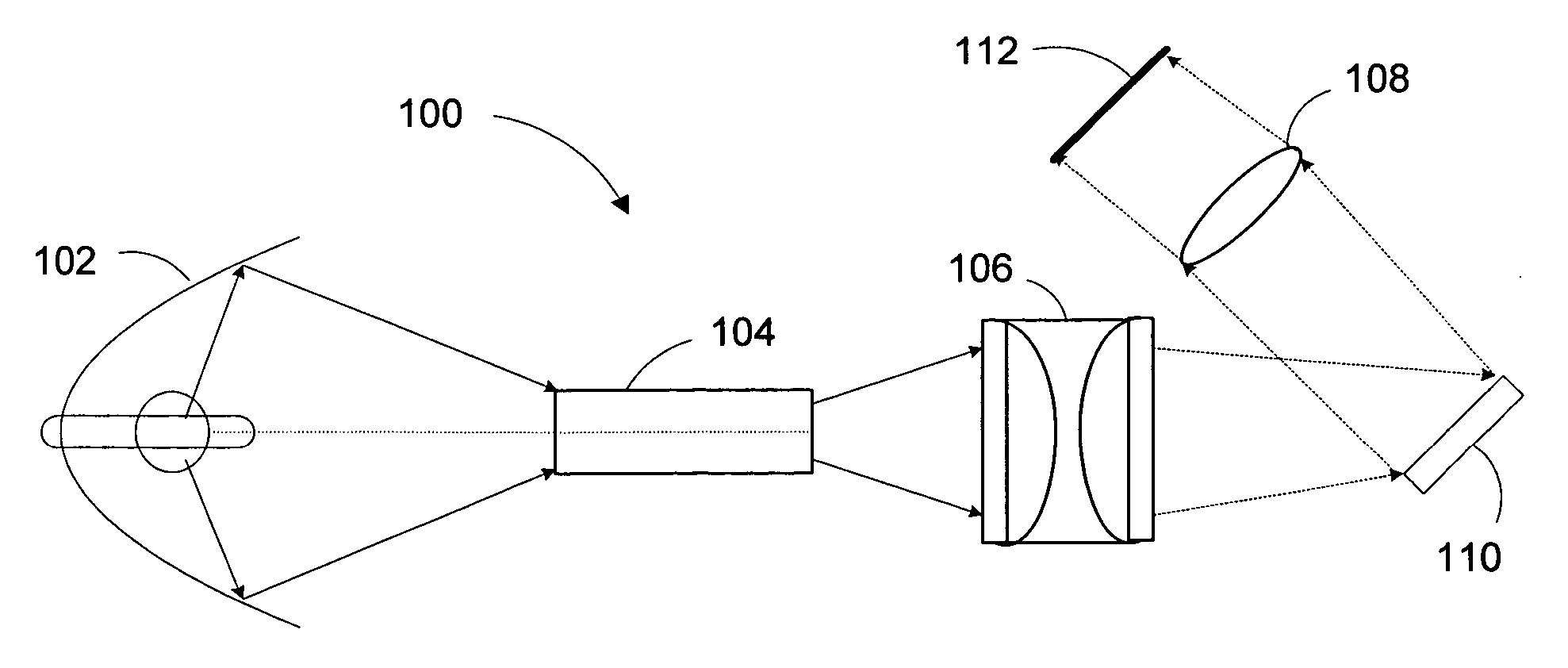
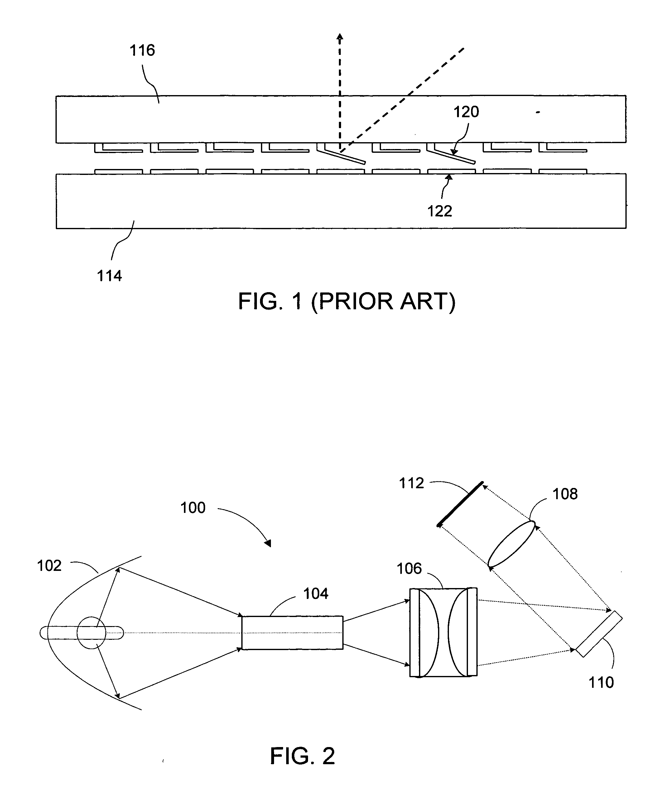
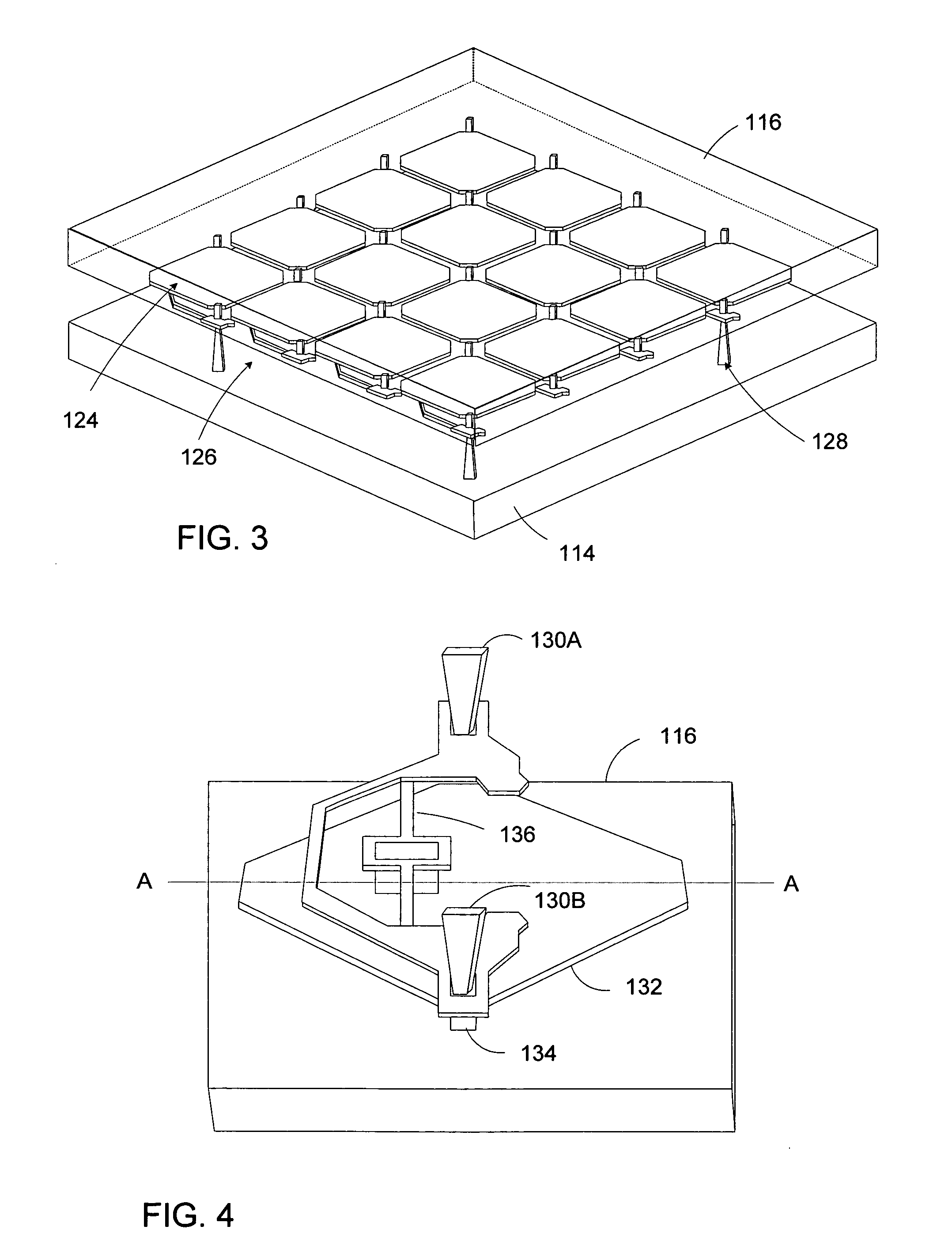
TECHNICAL FIELD OF THE INVENTION [0001] The present invention is related generally to the art of microelectromechanical systems, and, more particularly, to spatial light modulators having array of micromirrors and methods of making the same. BACKGROUND OF THE INVENTION [0002] Microstructures such as microelectromechanical systems are often fabricated on one or more substrates. These substrates may deform during fabrication or operation, causing degradation of the device performance or even device failure when the deformation exceeds a tolerable amount. Moreover, in those microstructures having multiple substrates, a uniform gap between two substrates is often required for ensuring desired functions or performance of the microstructure. [0003] As an example, FIG. 1 illustrates a portion of a micromirror array device which is a type of microelectromechanical device. An array of mirror plates such as mirror plate 120 is formed on glass substrate 116. The mirrors are operable to rotate ...

Claims


Application Information

Patent Timeline
IPC IPC(8): G02B26/00G02B26/08
CPCG02B26/0841Y10T156/10B81C3/001Y10S359/90
Inventor PATEL, SATYADEVHUIBERS, ANDREW G.RICHARDS, PETERTARN, TERRYDEHLINGER, DIETRICH
Owner TEXAS INSTR INC
Learn More