
Guided capture, creation, and seamless integration with scalable complexity of a clock specification into a design flow of an integrated circuit

Inactive Publication Date: 2005-12-08
BELL SEMICON LLC
View PDF3 Cites 17 Cited by
  • Summary
  • Abstract
  • Description
  • Claims
  • Application Information

AI Technical Summary

Benefits of technology

[0012] The tool, method, and program product may further restrict or hide clocking parameters not affecting nor affected by the user choices.

Problems solved by technology

The tool, method, and program product may further restrict or hide clocking parameters not affecting nor affected by the user choices.

Method used


Image

  • Guided capture, creation, and seamless integration with scalable complexity of a clock specification into a design flow of an integrated circuit
  • Guided capture, creation, and seamless integration with scalable complexity of a clock specification into a design flow of an integrated circuit
  • Guided capture, creation, and seamless integration with scalable complexity of a clock specification into a design flow of an integrated circuit

Examples


Embodiment Construction

in conjunction with the accompanying figures.

BRIEF DESCRIPTION OF THE DRAWINGS

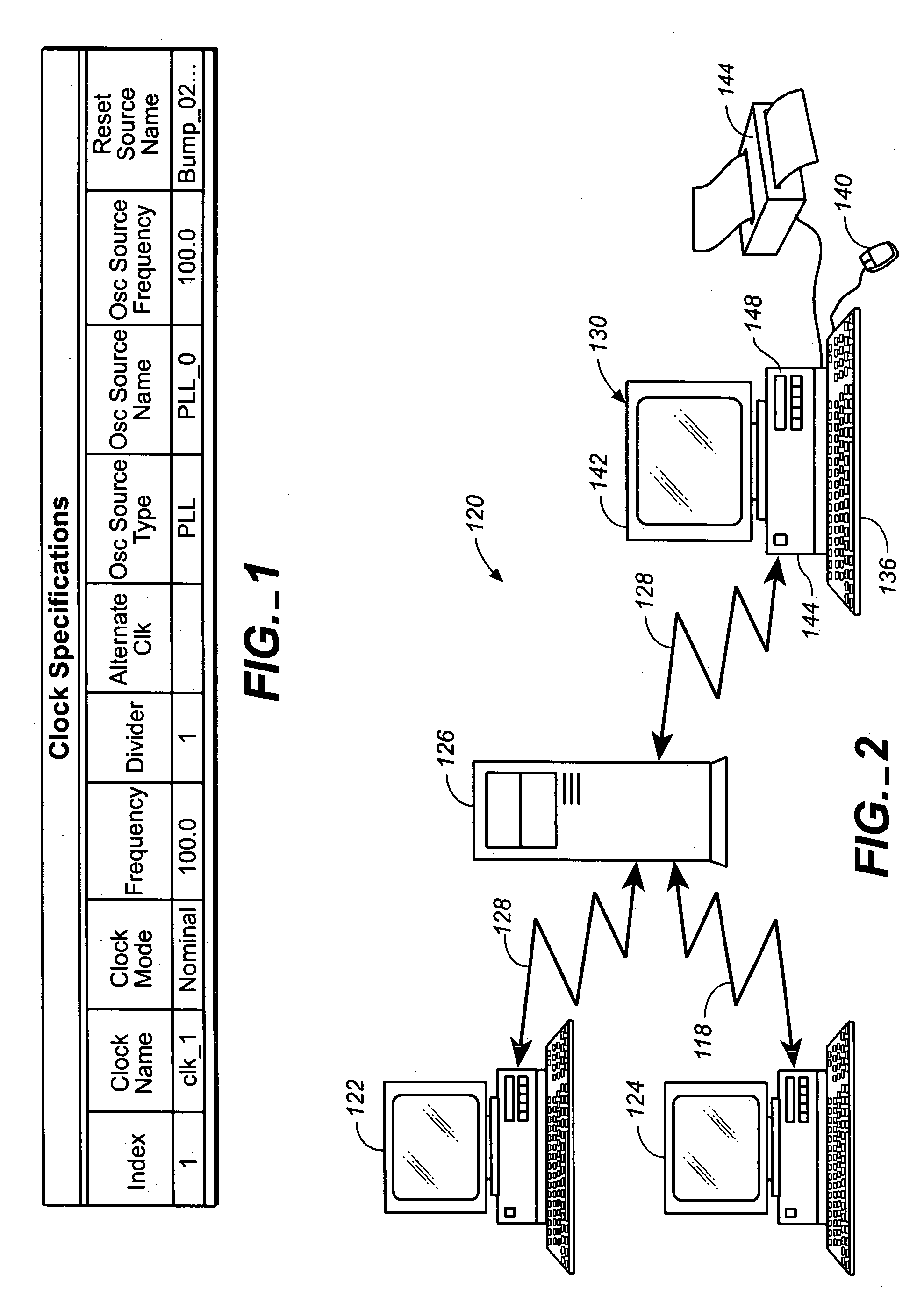
[0015]FIG. 1 is a simplified table specifying a clock.

[0016]FIG. 2 is block diagram of a networked computer system in which the clock specification, creation, and integration tool of the invention can be implemented.

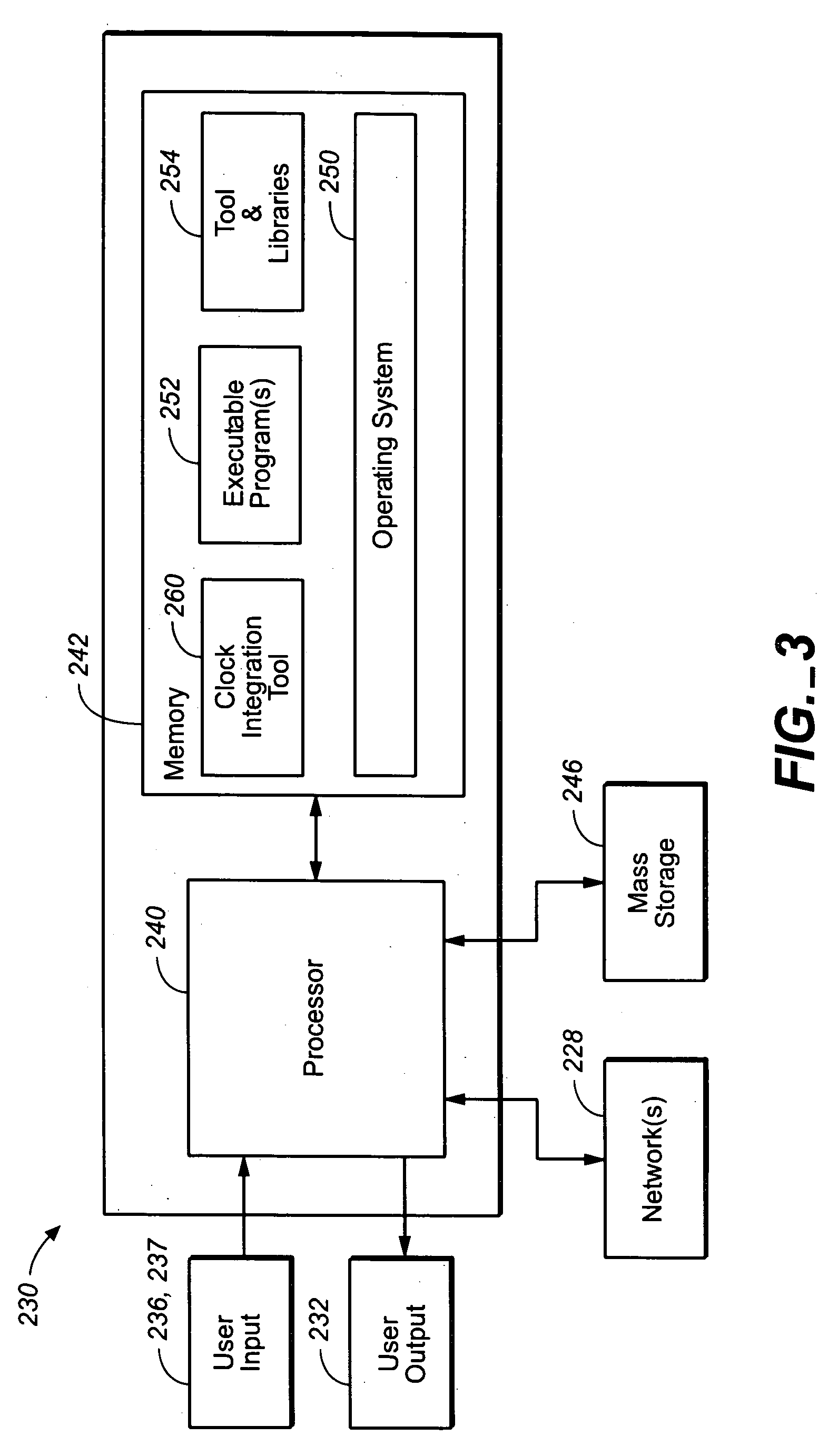
[0017]FIG. 3 is a simplified block diagram of the functional components within a computer workstation to which an integrated circuit developer may access and use the clock specification, creation, and integration tool in accordance with an embodiment of the invention.

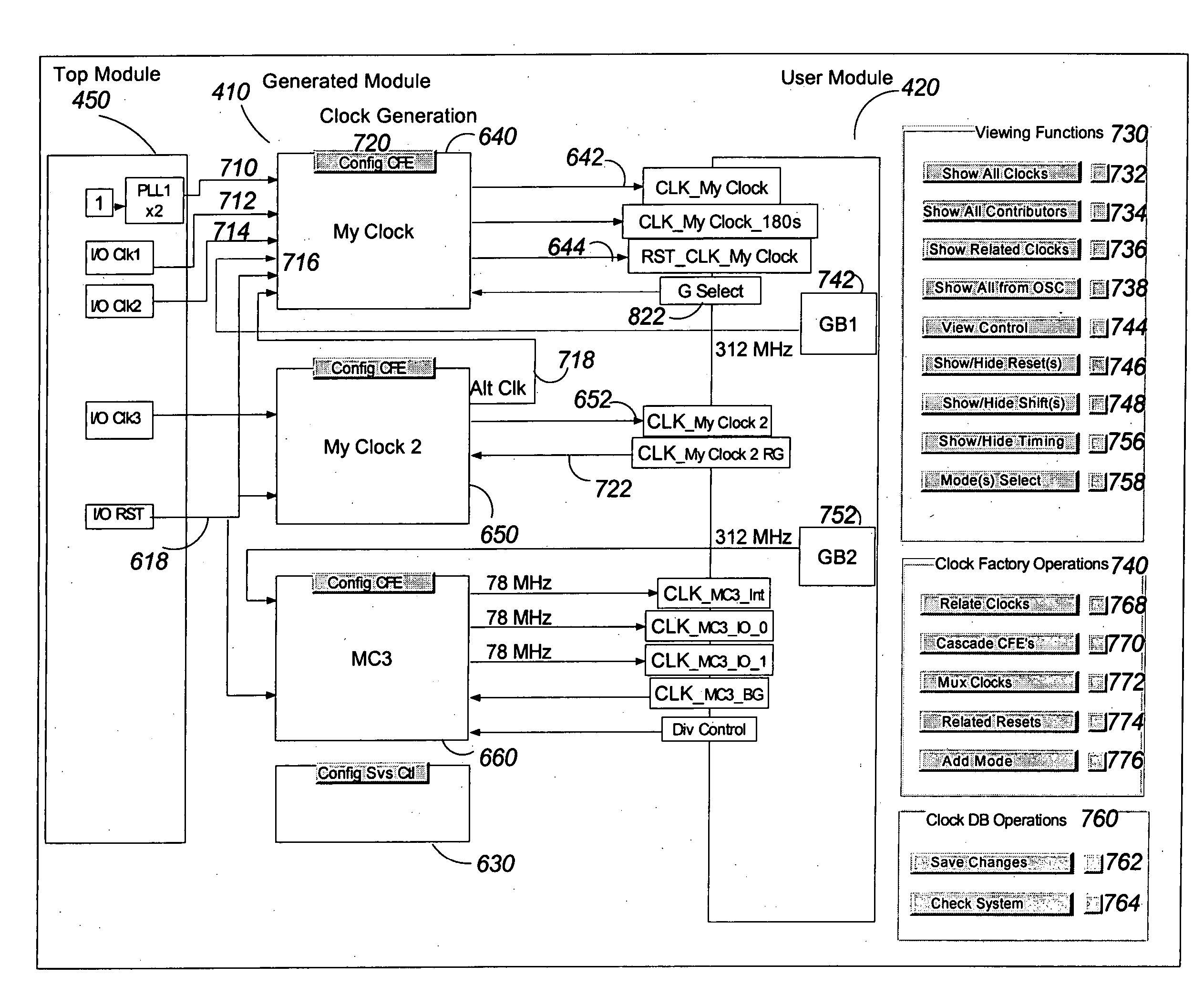
[0018]FIG. 4 is a simplified block diagram of a semiconductor platform having a number of components, each of which will probably have to be considered in terms of clocking, the clocks created and integrated according to an embodiment of the invention.

[0019]FIG. 5 is a simplified diagram illustrating the hierarchy of register transfer level logic of a semiconductor platform description usable by the clock specification, creati...


PUM


Abstract

A clock integration method, tool, and a computer program product that captures, creates, and seamlessly integrates a clock specification to achieve a correct-by-construction design flow of a semiconductor product, such as an ASIC, from a partially manufactured semiconductor platform. The clocking elements of the design flow are combined and displayed to a chip designer in a plurality of context-driven user interfaces and views. Within each view, the details of the clock specification are presented in the context of the information to guide a chip designer to make relevant and correct determinations, e.g., if the context is a high level overview of the logic of the intended semiconductor product, then only the high level parameters, such as source, frequency, path of the clocks signals through the high level modules, etc. are seen. When a chip designer wants more or less detailed information, she / he need only zoom in / zoom out through the plurality of views of the design flow. Each view can combine the logical, structural, architectural, cost, timing, and other features of the clock in a particular context. A user can zoom in all the way to select and manipulate the circuit elements of a PLL, a clock factory element, etc. as in the creation or generation of a clock for the intended semiconductor product. The user can then zoom out and the clock integration method and tool herein determines how changes in selected muxed clock signals and / or elements affect other clocks in the same or other modules and / or the same clock in other modules. Creating, inserting, and integrating clocks for a complex integrated circuit has never been easier.

Description

RELATED APPLICATIONS [0001] This application for an invention relates to U.S. Provisional Application Ser. No. 60 / 579,922 entitled RULES AND DIRECTIVES FOR VALIDATING CORRECT DATA USED IN THE DESIGN OF SEMICONDUCTOR PRODUCTS filed 15 Jun. 2004, and U.S. patent application Ser. No. ______ entitled RULES AND DIRECTIVES FOR VALIDATING CORRECT DA TA USED IN THE DESIGN OF SEMICONDUCTOR PRODUCTS, LSIL Docket 04-0977 filed 20 Dec. 2004 (referred to herein as a component of the TOOLS); it also relates to U.S. patent application filed on 6 May 2004 Ser. No. 10 / 840,534 entitled ASSURING CORRECT DA TA ENTRY TO GENERATE VIEWS FOR A SEMICONDUCTOR PLATFORM (referred to herein as a component of the TOOLS); and to U.S. Provisional Application Ser. No. 60 / 577,356 filed 3 Jun. 2004 and U.S. patent application Ser. No. ______, LSIL Docket No. 04-0824 entitled LANGUAGE AND TEMPLATE FOR USE IN THE DESIGN OF SEMICONDUCTOR PRODUCTS (referred to herein as a component of the TOOLS) filed 20 Dec. 2004, all a...

Claims


Application Information

Patent Timeline
IPC IPC(8): G06F1/04G06F9/44G06F9/45G06F17/50
CPCG06F9/453G06F1/04
Inventor BYRN, JONATHANLINDBERG, GRANT
Owner BELL SEMICON LLC
Learn More