Organic electroluminescent device, manufacturing method therefor, and electronic devices therewith
a technology of electroluminescent devices and organic membranes, applied in the direction of organic semiconductor devices, identification means, instruments, etc., can solve the problems of uneven chrominance, uneven thickness of organic membranes within pixels or among pluralities of pixels, and inability to evenly occupy pixels in both x and y directions, so as to achieve uniform chrominance and uniform displaying performance. , the effect of uneven luminan
- Summary
- Abstract
- Description
- Claims
- Application Information
AI Technical Summary
Benefits of technology
Problems solved by technology
Method used
Image
Examples
first embodiment
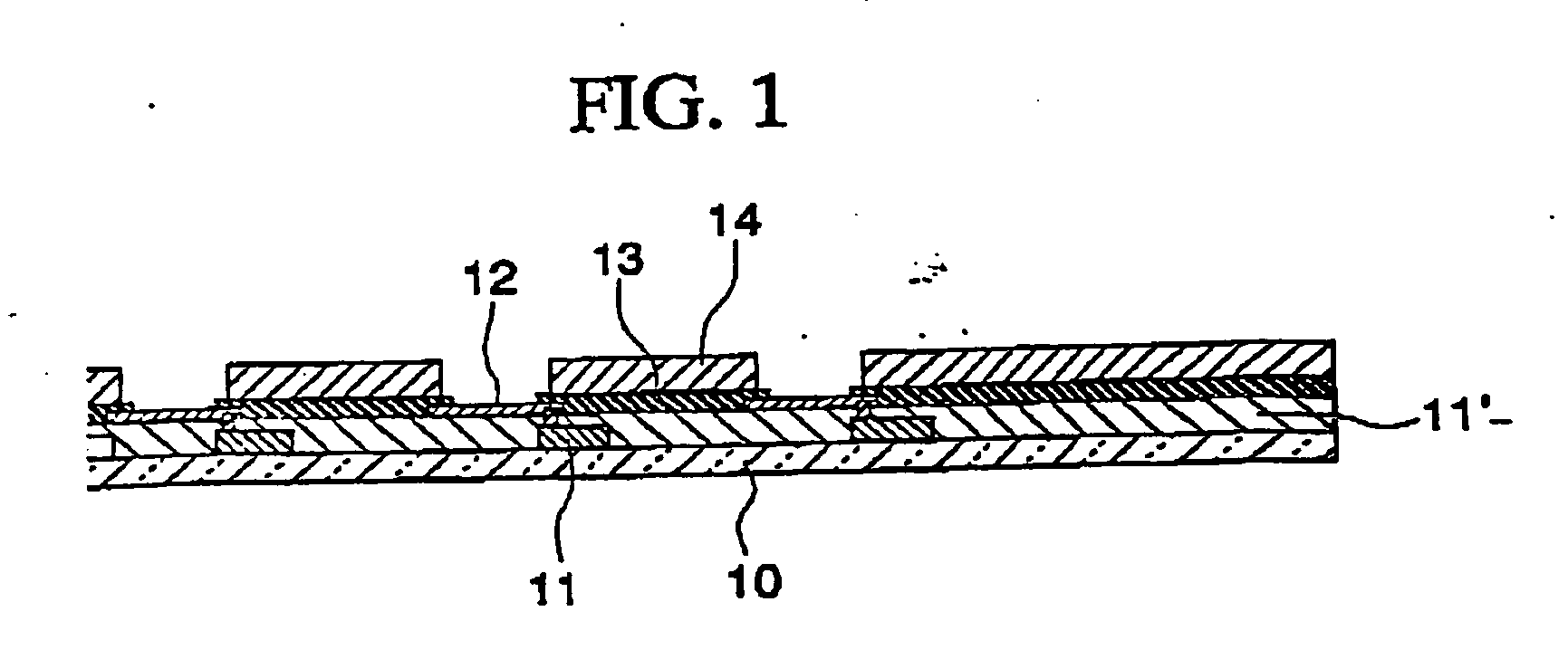
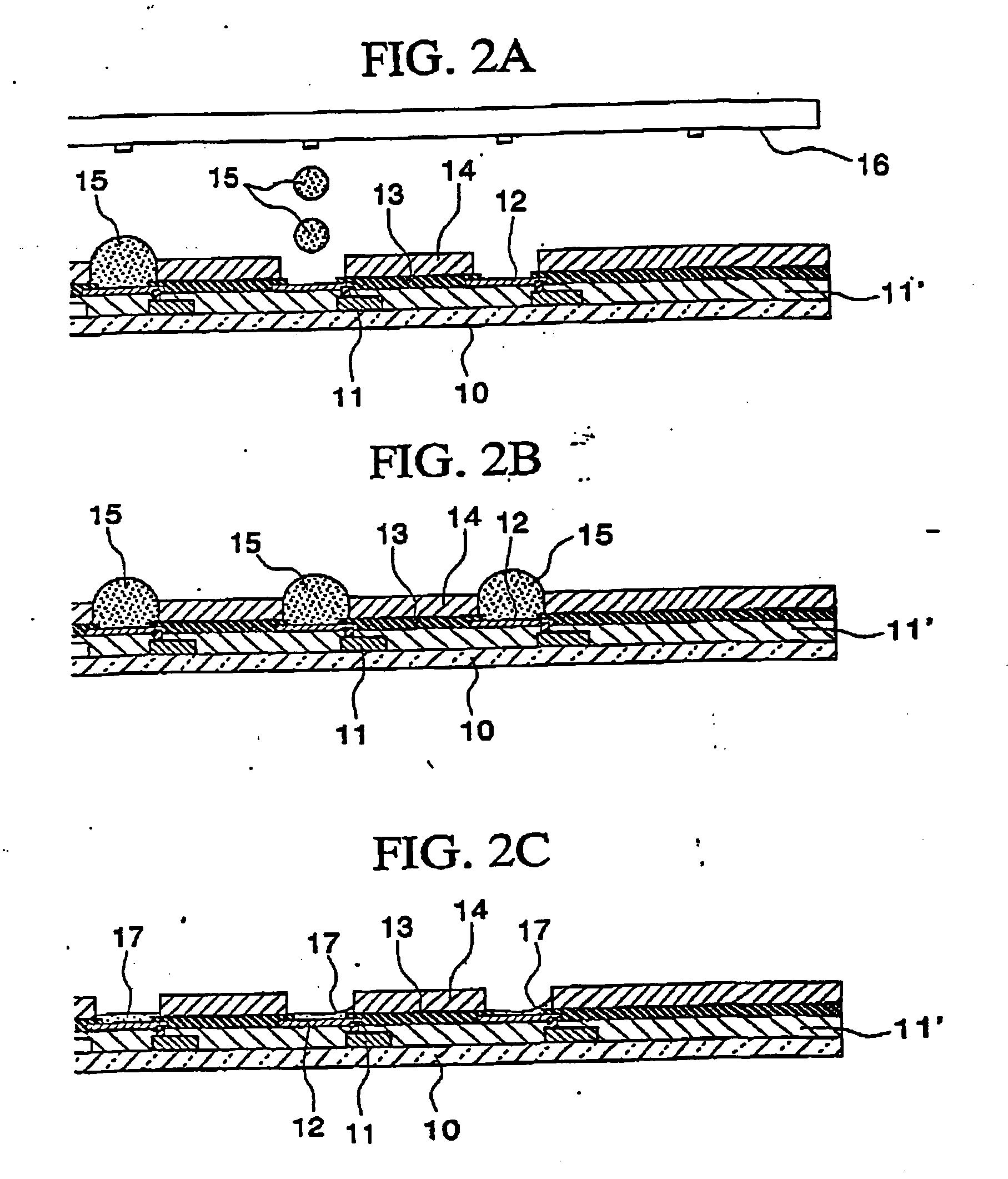
[0064] The substrate used in the first embodiment is a 2-inch TFT substrate in which circular pixels having diameters of 30 μm are disposed at a pitch of 70.5 μm in both X and Y directions. This TFT substrate includes a glass substrate 25 and a circuit element portion 26′ having TFTs 26 formed on the glass substrate. FIG. 3A is a partial cross-sectional view (along the X direction) of the right edge portion of the TFT substrate. Transparent electrodes 27 made of ITO are formed on the circuit element portion 26′ and banks including two layers including SiO2 banks 28 and polyimide banks 29 are constructed on the circuit element portion 26′ so as to divide the transparent electrodes 27. The SiO2 banks 28 are manufactured in a pattern by photo-etching after forming a 150 nm thick TEOS (tetraethylorthosilicate) layer by CVD (Chemical Vapor Deposition). The polyimide banks 29, which are 2 μm thick, are formed on the SiO2 banks 28 through the steps of coating a photosensitive polyimide on ...
second embodiment
[0073] In the second embodiment shown in FIGS. 4A and 4B, a TFT substrate in which a dummy area B is disposed around an effectively optical area A is used, as in the first embodiment. This TFT substrate includes a glass substrate 25 and a circuit element portion 26′ having TFTs 26 formed on the glass substrate. Transparent electrodes 27 made of ITO are formed on the circuit element portion 26′ and banks including two layers including SiO2 banks 28 and polyimide banks 29 are constructed on the circuit layer 26′ so as to divide the transparent electrodes 27. Thus, display pixels 42 are formed in the effectively optical area A.
[0074] A SiO2 membrane 28′ extending from the SiO2 banks is formed in the dummy area B. The dummy pixels 43 having the same shape as that of the display pixels 42 and disposed at the same pitch as that at which the display pixels 42 are disposed are defined by polyimide banks 40. FIG. 4A is a partial cross-sectional view of the night edge portion of the substrat...
third embodiment
[0077] In the third embodiment shown in FIGS. 5A to 5D, a TFT substrate in which a dummy area B is disposed around an effectively optical area A, is used, as in the first embodiment. This TFT substrate includes a glass substrate 25 and a circuit element portion 26′ having TFTs 26 formed on the glass substrate, as shown in FIG. 5A. Transparent electrodes 27 made of ITO are formed on the circuit element portion 26′ and banks including two layers including SiO2 banks 28 and polyimide banks 29 are constructed on the circuit element portion 26′ so as to divide the transparent electrodes 27. Thus, display pixels 42 are formed in the effectively optical area A.
[0078] On the circuit element portion 26′ in the dummy area B, dummy pixels 44 having the same shape and disposed at the same pitch as the display pixels 42 are only defined by polyimide banks 29. FIG. 5A is a partial cross-sectional view of the right edge portion of the substrate.
[0079] The polyimide banks 29 are made to be ink-re...
PUM
 Abstract
Description
Claims
Application Information
 - R&D
- Intellectual Property
- Life Sciences
- Materials
- Tech Scout
- Unparalleled Data Quality
- Higher Quality Content
- 60% Fewer Hallucinations
Browse by: Latest US Patents, China's latest patents, Technical Efficacy Thesaurus, Application Domain, Technology Topic, Popular Technical Reports.
© 2025 PatSnap. All rights reserved.Legal|Privacy policy|Modern Slavery Act Transparency Statement|Sitemap|About US| Contact US: help@patsnap.com


