
Alignment system and method and device manufactured thereby

a technology of alignment system and alignment method, which is applied in the direction of electrical equipment, instruments, printing, etc., can solve the problems of overlay errors between layers on the substrate, substrate or a device finally cut out of the substrate may be rejected, and the superposition error of two images is generally called an overlay error, so as to simplify the selection process

Active Publication Date: 2005-11-17
ASML NETHERLANDS BV
View PDF3 Cites 22 Cited by
  • Summary
  • Abstract
  • Description
  • Claims
  • Application Information

AI Technical Summary

Benefits of technology

[0015] Therefore, one aspect of an embodiment of the present invention to simplify the process of selecting a suitable set of mark pairs among a predetermined set of alignment marks.
[0024] They need to select a set of overlay metrology targets (the overlay in both X and Y direction are measured on the same target) which will give them an accurate and reliable measurement result, representing the overlay achieved on the substrate. The accuracy and reliability increase by performing more overlay measurements on different overlay metrology targets, while measuring more overlay metrology targets impacts productivity. This means that the time needed to measure the overlay metrology marks should be as short as possible in order to reduce loss of throughput.
[0025] The number of overlay metrology targets per field and their location in the field can be constant, e.g., 4 overlay metrology targets per field, or the number of overlay metrology targets and their location can change from field to field, depending on an underlying wafer model. In this case the number of overlay metrology targets to be measured can be reduced, while the accuracy of the measurement is hardly affected, thus increasing productivity.
[0027] Therefore, one aspect of an embodiment of the present invention to simplify the process of selecting a suitable set of overlay metrology targets among a predetermined set of overlay metrology targets.

Problems solved by technology

If a mark on a substrate is not correctly aligned to the corresponding reference point in the mask this alignment error will cause an error in the super-positioning of two images exposed on successive layers on the substrate.
This error in the super-positioning of two images is generally called an overlay error.
If a large overlay error occurs, the substrate or a device finally cut out of the substrate may be rejected during a quality inspection.
This may cause overlay errors between layers on the substrate.
Not all these alignment marks will be used since not all of them are,,e.g., suitable to be used or using them all will take too much time without improving the accuracy of the measurement significantly.
However, these operators are confronted with several problems:
A special problem is Wafer Capture.
Moreover, a generic problem for operators is that they need to optimize a selected mark-layout for best overlay and also for maximum productivity.

Method used


Image

  • Alignment system and method and device manufactured thereby
  • Alignment system and method and device manufactured thereby
  • Alignment system and method and device manufactured thereby

Examples


embodiments

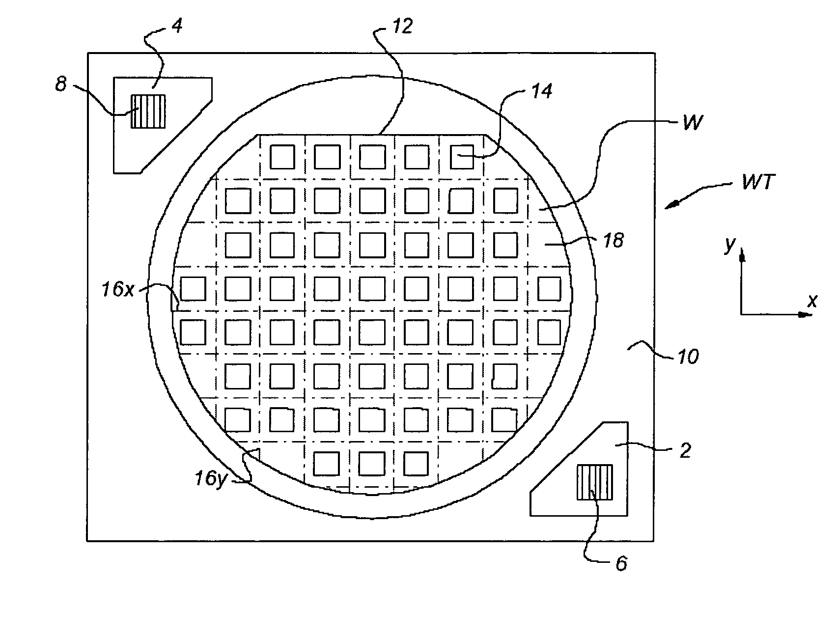
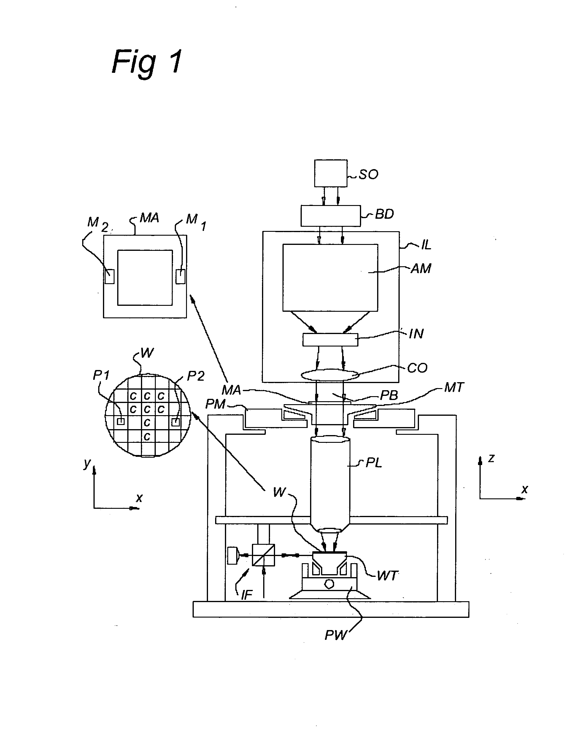
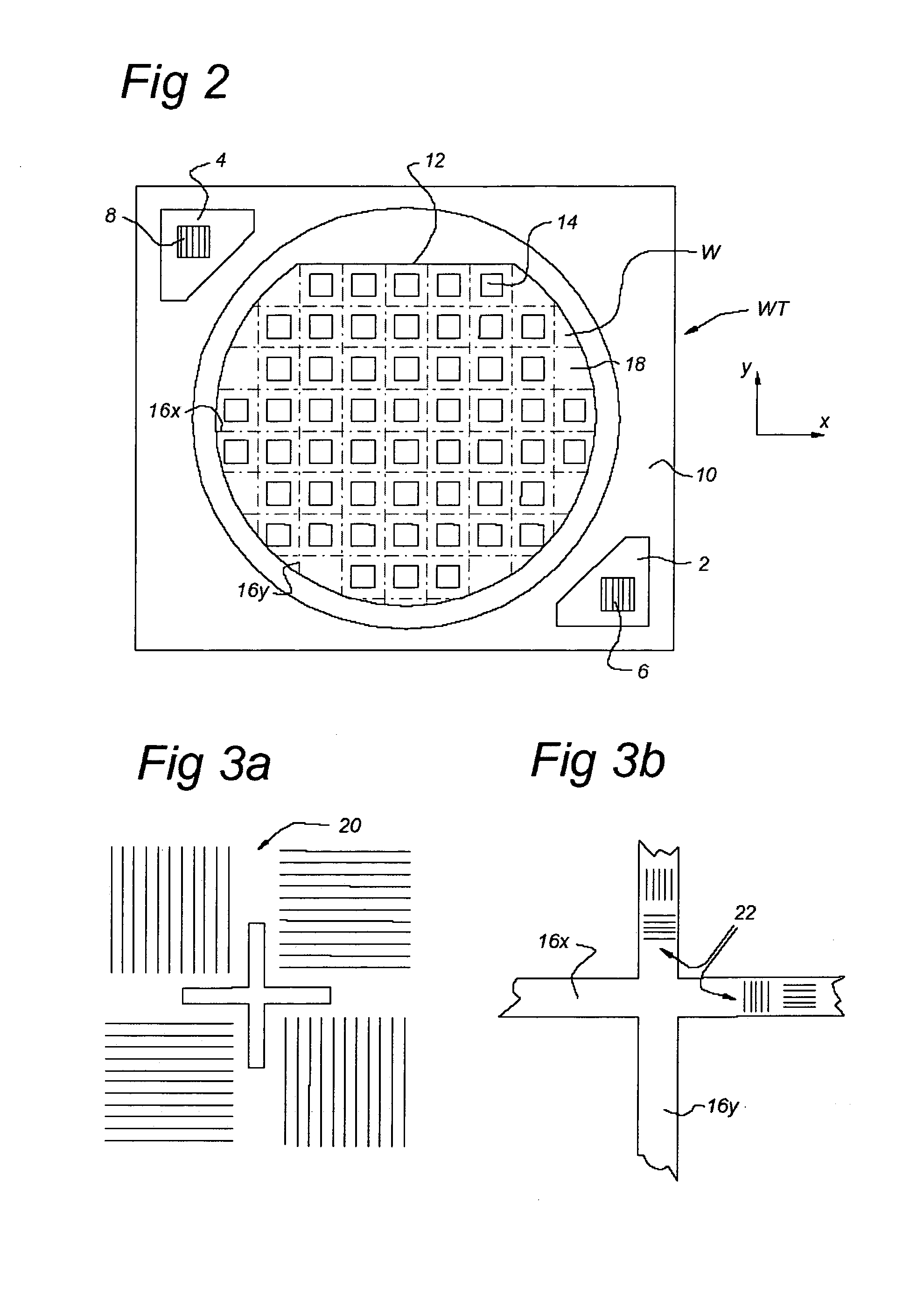
[0047]FIG. 1 schematically depicts a lithographic apparatus according to a particular embodiment of the invention. The apparatus comprises: [0048] an illumination system (illuminator) IL for providing a projection beam PB of radiation (e.g., visible light, UV radiation or radiation with even lower frequencies). [0049] a first support structure (e.g., a mask table) MT for supporting patterning device (e.g., a mask) MA and connected to first positioner PM for accurately positioning the patterning device with respect to item PL; [0050] a substrate table (e.g., a wafer table) WT for holding a substrate (e.g., a resist-coated wafer) W and connected to second positioner PW for accurately positioning the substrate with respect to item PL; and [0051] a projection system (e.g., a refractive projection lens) PL for imaging a pattern imparted to the projection beam PB by patterning device MA onto a target portion C (e.g., comprising one or more dies) of the substrate W.

[0052] As here depicted...


PUM


Abstract

An arrangement for and a method of automatically selecting substrate alignment marks on a substrate in a lithographic apparatus or overlay metrology targets in an overlay metrology apparatus. The apparatus has a processor and a memory connected to the processor. The memory stores locations of one or more sets of substrate alignment marks or overlay metrology targets available for selection and selection rules to select suitable substrate alignment marks or overlay metrology targets from this at least one set. The selection rules are based on experimental or theoretical knowledge about which substrate alignment mark or overlay metrology targets locations are optimal in dependence on one or more selection criteria.

Description

BACKGROUND OF THE INVENTION [0001] 1. Field of the Invention [0002] The present invention relates generally to alignment systems and more particularly their uses in lithographic apparatus or overlay measurement apparatus. [0003] 2. Description of the Related Art [0004] A lithographic apparatus is a machine that applies a desired pattern onto a target portion of a substrate. Lithographic apparatus can be used, for example, in the manufacture of integrated circuits (ICs). In that circumstance, a patterning device, which is alternatively referred to as a mask or a reticle, may be used to generate a circuit pattern corresponding to an individual layer of the IC, and this pattern can be imaged onto a target portion (e:g., comprising part of, one or several dies) on a substrate (e.g., a silicon wafer) that has a layer of radiation-sensitive material (resist). In general, a single substrate will contain a network of adjacent target portions that are successively exposed. Known lithographic...

Claims


Application Information

Patent Timeline
IPC IPC(8): G03F7/20G03B27/42H01L21/027
CPCG03F9/7046G03B27/42
Inventor TOLSMA, HOITE PIETER THEODOORNAVARRO Y. KOREN, RAMONSIMONS, HUBERTUS JOHANNES GERTRUDUSEDART, REMI DANIEL MARIELAM, PUI LENGHULSHOF, BERNARDUS JOHANNES ANTONIUSBOGERS, ROLAND ADRIANUS EMANUEL MARIA
Owner ASML NETHERLANDS BV
Learn More