
Method and apparatus for display panel drive

Active Publication Date: 2005-10-06
RENESAS ELECTRONICS CORP
View PDF3 Cites 24 Cited by
  • Summary
  • Abstract
  • Description
  • Claims
  • Application Information

AI Technical Summary

Benefits of technology

[0027] The fact that the drive sequence of an nth line out of the plurality of lines is different from that of an (n+1)th line out of the plurality of lines is effective for spatially distributing pixels experiencing increased changes of drive voltages thereacross. Additionally, the fact that the G pixels, each included within associated one of the first to Nth pixels sets, are driven (N+1)th earliest or later for each of the nth and (n+1)th line is effective for reducing uneven brightness due to the effects of the spectrum luminous efficacy characteristics of human vision.

Problems solved by technology

One issue caused by the increase in the number of the signal lines is difficulty in providing electrical connections between the signal lines and the display panel driver; the decrease in the intervals between adjacent signal lines undesirably makes it difficult to provide sufficient spacing between external wirings connected between the signal lines and the display panel driver.
Another issue is the increase in the number of amplifiers for driving the signal lines incorporated within the driver.
The increased number of amplifiers undesirably increases the size of the driver, and thus increases the cost.
The two known techniques, however, have a drawback that the drive voltage developed across the liquid crystal capacitor 12 within each pixel may be varied from the desired level after the associated signal line is placed into the high-impedance state, disconnected from the associated input terminal 14.
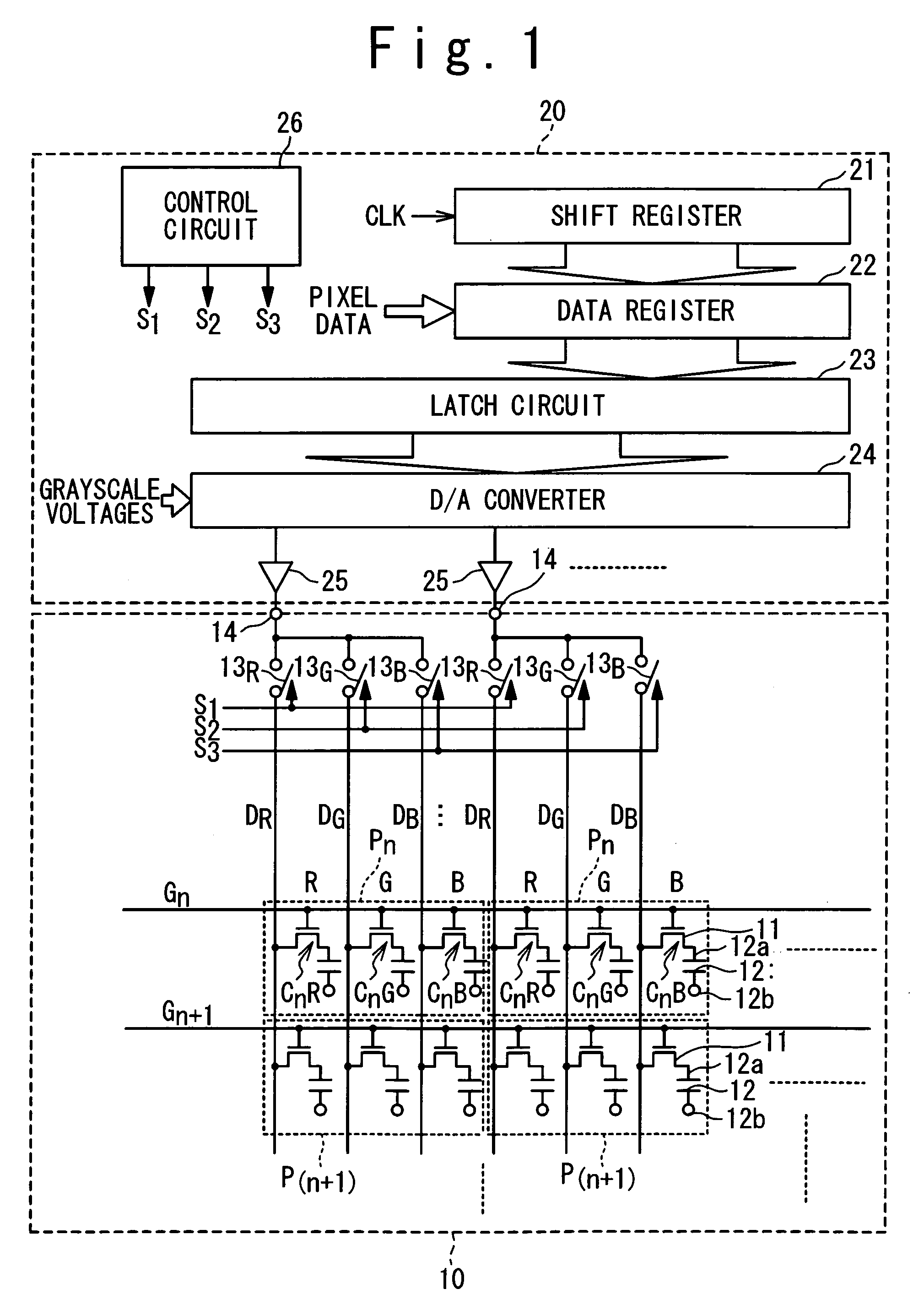
The first cause is leakage through TFTs within the switches 13 provided for switching the signal lines D. Referring to FIG. 1, the signal lines D are inevitably long, and thus have increased capacitance.
This requires the TFTs within the switches 13 to have increased drive ability for driving the signal lines D. Accordingly, the TFTs are designed to have an increased gate width and reduced gate length, and a small on-resistance; however, such designed TFTs suffer from increased leakage.
Such variation in the voltage at the signal line DR will result in a change in the drive voltage across the pixel.
The increase in the number of the signal lines for each amplifier undesirably causes increased change in the drive voltages.

Method used


Image

  • Method and apparatus for display panel drive
  • Method and apparatus for display panel drive
  • Method and apparatus for display panel drive

Examples


first embodiment

1. Structure of Display Device

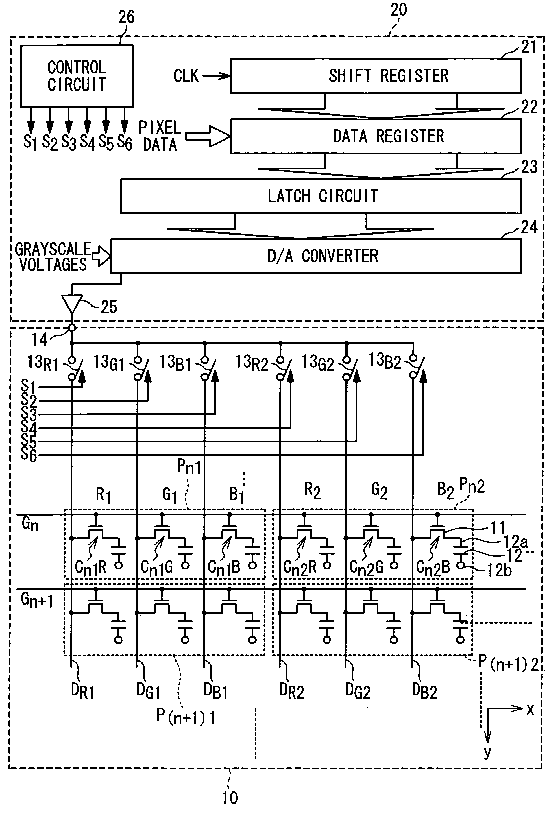
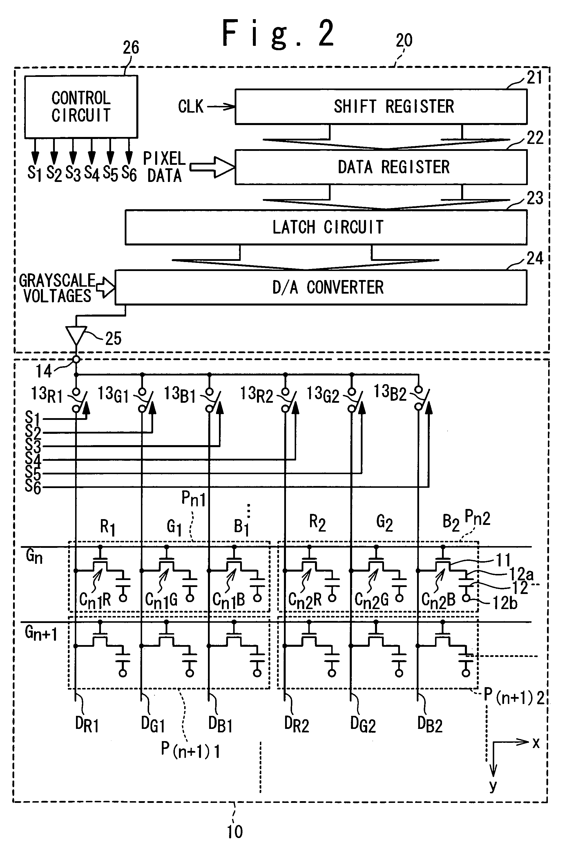
[0060] In a first embodiment, as shown in FIG. 2, a display panel driving method according to the present invention is employed in a display device designed to drive six signal lines in a time-divisional manner. The display device according to the first embodiment is almost similar in the arrangement to the display device shown in FIG. 1, except that the number of signal lines to be driven by a single amplifier is different. Like components shown in FIG. 2 are denoted by like numerals as those shown in FIG. 1. The display device in the first embodiment will schematically be described.

[0061] In this embodiment, the display device is composed of a liquid crystal panel 10 incorporating an array of pixels, and a driver 20 for driving the liquid crystal panel 10. The liquid crystal panel 10 includes a set of scanning lines G1, G2 . . . , signal lines DR1 and DR2 associated with red, signal lines DG1 and DG2 associated with green, and signal lines DB1 and ...

second embodiment

1. General Outline

[0120] A display panel driving method of the second embodiment of the present invention is illustrated in FIGS. 6A to 6C, 7A to 7C, 9A to 9C, 11, and 12, where examples of the drive sequence of each line are shown. In the second embodiment, the display panel driving method is modified from that of the first embodiment for driving a display panel in which the number of the pixel sets for each input terminal is 2×K, K being an integer equal to or more than 2; in other word, the display panel driving method of this embodiment addresses driving 6×K signal lines with a single amplifier in a time divisional manner.

[0121] The drive sequence of each line in the second embodiment is also determined so as to satisfy the requirements described in the first embodiment. For example, the ordinal number of each pixel in a specific line is determined as being different from that of the corresponding pixel in the adjacent line. Additionally, the ordinal numbers of the G pixels a...

third embodiment

1. Structure of Display Device

[0192] A third embodiment of the present invention will be described in conjunction with a display device, shown in FIG. 13, where three signal lines are time-divisionally driven by the foregoing display panel driving method. In this embodiment, a liquid crystal display panel 10′ is differentiated from the display panel 10 shown in FIG. 2 by the fact that the pixels within the pixel set Pi1 are connected to a different input terminals 14 from that connected with the pixels within the pixel unit Pi2. It is hence assumed that the input terminal connected with the pixel unit Pi1 is denoted by 141, while the input terminal connected with the pixel unit Pi2 is denoted by 142. Also, an amplifier connected to the input terminal 141 is denoted by 251, while another amplifier connected to the input terminal 142 is denoted by 252. More particularly, the R pixel Ci1R, the G pixel Ci1G, and the B pixel Ci1B within the pixel set Pi1, are connected through three sw...


PUM


Abstract

A method is provided for driving a display panel including N×3 pixels arranged along each of a plurality of lines extending in a scanning line direction with N being an integer equal to or more than 2, the N×3 pixels constituting first to Nth pixel sets each comprising an R pixel associated with red, a G pixel associated with green, and a B pixel associated with blue. The method is composed of time-divisionally driving the N×3 pixels positioned in each of the plurality of lines. A drive sequence of an nth line out of the plurality of lines is different from that of an (n+1)th line out of the plurality of lines, the (n+1)th line being adjacent to the nth line. The G pixels, each included within associated one of the first to Nth pixels sets, are driven (N+1)th earliest or later for each of the nth and (n+1)th line.

Description

BACKGROUND OF THE INVENTION [0001] 1. Field of the Invention [0002] The present invention relates to display panel driving methods, display panel drivers, and display panel driving programs. Particularly, the present invention relates to driving techniques for time-divisionally driving two or more signal lines (data lines) within a display panel with a single amplifier. [0003] 2. Description of the Related Art [0004] As display panels have been shifted to higher resolution, signal lines (or data lines) within display panels are significantly increased in the number, and thus the intervals between adjacent signal lines are significantly decreased. One issue caused by the increase in the number of the signal lines is difficulty in providing electrical connections between the signal lines and the display panel driver; the decrease in the intervals between adjacent signal lines undesirably makes it difficult to provide sufficient spacing between external wirings connected between the si...

Claims


Application Information

Patent Timeline
IPC IPC(8): G09G3/20G02F1/133G09G3/36G09G5/00G09G5/02
CPCG09G3/3648G09G3/3688G09G2320/0219G09G2310/0297G09G2320/0209G09G2310/027
Inventor NOSE, TAKASHITOEDA, MASAHIRO
Owner RENESAS ELECTRONICS CORP
Learn More