
Method and system for correcting a fault in a semiconductor manufacturing system

Inactive Publication Date: 2005-09-29
SUPPORT RESOURCES HLDG
View PDF15 Cites 10 Cited by
  • Summary
  • Abstract
  • Description
  • Claims
  • Application Information

AI Technical Summary

Benefits of technology

[0007] Accordingly, one aspect of the present invention is to reduce or eliminate any or all of the above-described problems.
[0008] Another object of the present invention is to reduce service costs and maximize operating efficiency in the maintenance of a semiconductor manufacturing facility.

Problems solved by technology

Maintaining a semiconductor manufacturing facility is a time-consuming and expensive procedure that involves collaboration between equipment manufacturers and the manufacturing facility.
The inefficient interaction between a semiconductor equipment manufacturer and a semiconductor manufacturing facility can result in facility downtimes that add to the overall operational cost, as well as excessive consumption of engineering time and hardware replacements.
As a result, these service models exhibit a lack of communication of data between one another, significant overlap leading to redundancies, as well as establishing virtual boundaries within the structure designed to facilitate equipment service.
The present inventors have recognized that this use of independent service models leads to increased service costs and reduced operating efficiency.

Method used


Image

  • Method and system for correcting a fault in a semiconductor manufacturing system
  • Method and system for correcting a fault in a semiconductor manufacturing system
  • Method and system for correcting a fault in a semiconductor manufacturing system

Examples


Embodiment Construction

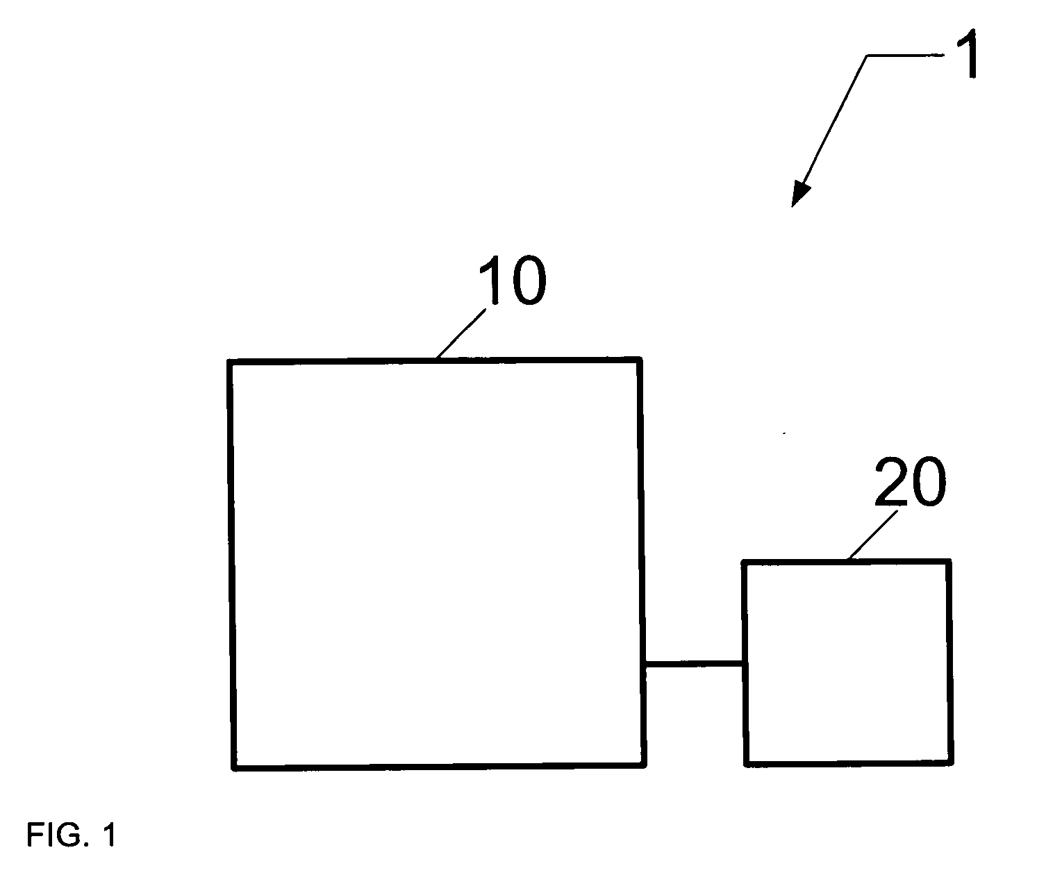
[0029] Referring now to the drawings wherein like reference numerals designate identical or corresponding parts throughout the several views, FIG. 1 presents a processing system 1 for semiconductor manufacturing. The processing system 1 includes a process tool 10 configured to perform a process on a substrate, and a control system 20 coupled to the process tool 10 and configured to perform a service function for correcting the process tool 10 using the service activity data. The service function performed by the control system may provide service action data useful to a service operator in correcting a fault in the process tool 10, or may provide automatic control of the process tool in order to correct the fault. According to one embodiment, the control system 20 stores service activity data used to perform service functions and correct a fault in the process tool 10.

[0030] The control system 20 can be directly coupled to the process tool 10, or it may be coupled to the process to...


PUM


Abstract

A method and system for correcting a fault in a semiconductor manufacturing system is described. Fault correction for a service component is achieved using an interactive case study with a service operator. The interactive case study can identify one or more cases where the current service activity data substantially matches past service activity data, and utilize this correlation to assist the service operator in conducting the service component repair. If necessary, the interactive case study can identify one or more tests to perform in order to narrow down the number of matching cases. As tests are performed and results are retrieved by the interactive case study, the number of matching cases is reduced. For instance, the interactive case study can assist in identifying a manufacturing system part to replace in a manufacturing system tool in order to correct the problem.

Description

CROSS-REFERENCE TO RELATED APPLICATION [0001] This application is related to co-pending U.S. patent application Ser. No. 10 / XXX,XXX, entitled “Activity management system and method of using”, Attorney docket no. 250049US6 YA / TEA-011, filed on Mar. 15, 2004. The entire contents of this application are herein incorporated by reference in their entirety.BACKGROUND OF THE INVENTION [0002] 1. Field of the Invention [0003] The present invention relates to a method and system for correcting a fault in a semiconductor manufacturing system, and, more particularly, to a method of correcting a fault using an interactive case study with a service operator. [0004] 2. Description of Related Art [0005] Maintaining a semiconductor manufacturing facility is a time-consuming and expensive procedure that involves collaboration between equipment manufacturers and the manufacturing facility. The inefficient interaction between a semiconductor equipment manufacturer and a semiconductor manufacturing faci...

Claims


Application Information

Patent Timeline
IPC IPC(8): G05B19/418H01L21/66
CPCG05B19/4184G05B2219/31357G05B2219/32408G05B2219/45031G06Q10/06G06Q10/0637H01L2924/0002G06Q10/20H01L22/20H01L2924/00Y02P90/02H01L21/00
Inventor KAUFFMAN, ERICBROWN, PAUL
Owner SUPPORT RESOURCES HLDG
Learn More