
Method and apparatus for depositing material with high resolution

a technology of high resolution and material, applied in the field of electronic devices, can solve the problem of limited resolution that may be achieved with such masks, and achieve the effect of high resolution and high resolution

Inactive Publication Date: 2005-09-29
THE TRUSTEES FOR PRINCETON UNIV
View PDF7 Cites 10 Cited by
  • Summary
  • Abstract
  • Description
  • Claims
  • Application Information

AI Technical Summary

Benefits of technology

"The patent describes a device that can deposit and remove material with high precision. It includes a base and a reservoir with a small opening. The device can be attached to a position control apparatus that can accurately position the base. It can also be coupled to an energy application apparatus that can apply energy to the material. The device can be used to deposit or remove material from a substrate with a resolution of a few molecules across."

Problems solved by technology

However, the resolution that may be achieved with such masks is limited due to a number of factors, including the resolution to which a mask may be reliably fabricated, the buildup of organic material on the mask, and the diffusion of organic material in between the mask and the substrate over which it is being deposited.

Method used


Image

  • Method and apparatus for depositing material with high resolution
  • Method and apparatus for depositing material with high resolution
  • Method and apparatus for depositing material with high resolution

Examples


Embodiment Construction

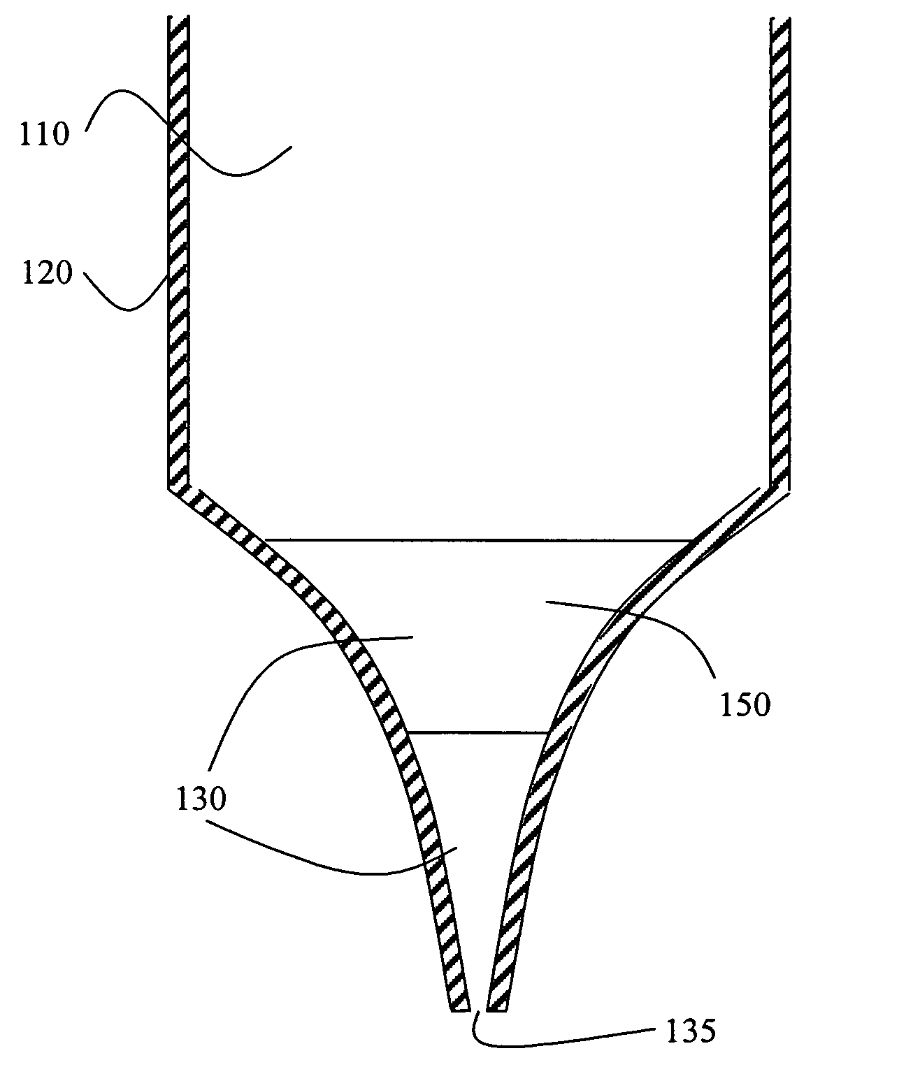
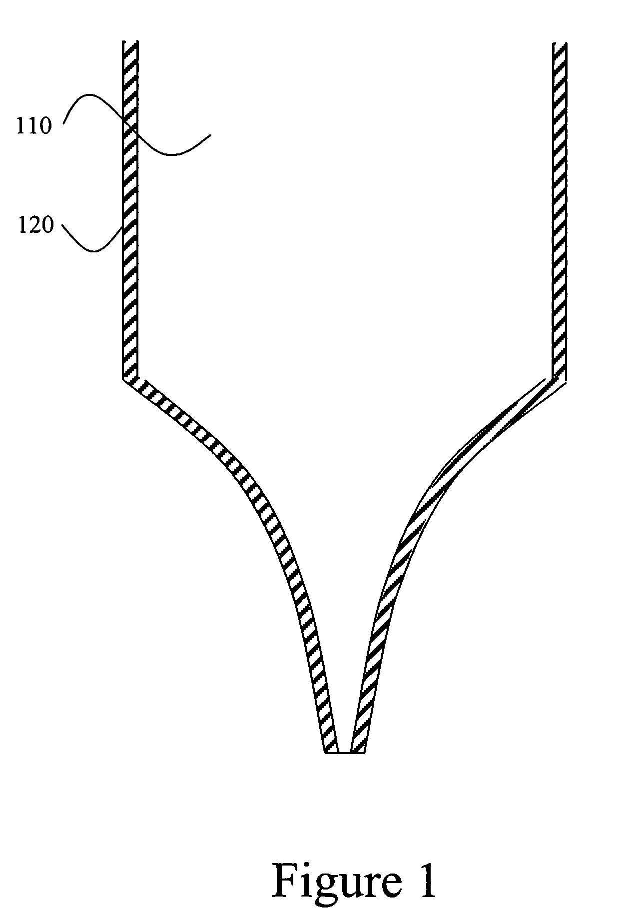
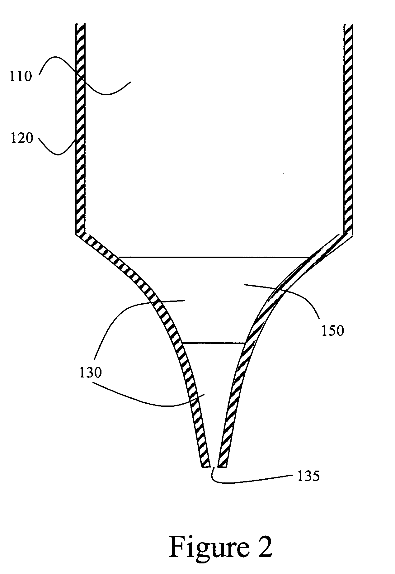
[0012]FIGS. 1 and 2 illustrate a process for fabricating a device for depositing organic materials in accordance with an embodiment of the invention. A base 110 having a tip with a very small largest dimension is made. Preferably, the dimension is about 50 nm or less. Depending upon the size of the feature that will be fabricated with the device, a different dimension may be used. One structure suitable for use as a base is a near field scanning optical microscope (“NSOM”) tip. NSOM or atomic force microscopy (“AFM”) tips suitable for use as a base may be obtained commercially from Veeco Instruments, Inc. of Freemont, Calif. or Nanonics Imaging Ltd. of Jerusalem, Israel. One method of making base 110 is to pull an optical fiber. Any optical fiber having an end that is narrowed by pulling may be referred to as a “pulled fiber.” Base 110 is then coated with a cladding 120. Preferred cladding materials include metals and metal oxides. Gold is a preferred cladding material. Preferred me...


PUM

PropertyMeasurementUnit
diameteraaaaaaaaaa
diameteraaaaaaaaaa
diameteraaaaaaaaaa

Abstract

A device is provided. The device includes a base, and a reservoir disposed in the base. The reservoir is defined by a cladding and the base, and has an opening with a largest dimension of about 200 nm or less, more preferably 100 nm or less, and most preferably 60 nm or less. A material may be disposed within the reservoir. The base may be attached to a position control apparatus that may control the position of the base with an accuracy on the order of nanometers. The position control apparatus may include an atomic force microsope and / or a near field scanning optical microscope. The base may also be coupled to an energy application apparatus that may apply energy to the material. The device may be used to deposit material onto a substrate with a very high resolution, on the order of a few molecules across. The device may also be used to remove material from a substrate with a very high resolution by transmitting energy through the base. A device used for such removal may or may not include a reservoir.

Description

FIELD OF THE INVENTION [0001] The present invention relates to electronic devices, and more specifically to a method and apparatus for fabricating such devices with features as small as several molecules across. BACKGROUND [0002] Opto-electronic devices that make use of organic materials are becoming increasingly desirable for a number of reasons. Many of the materials used to make such devices are relatively inexpensive, so organic opto-electronic devices have the potential for cost advantages over inorganic devices. In addition, the inherent properties of organic materials, such as their flexibility, may make them well suited for particular applications such as fabrication on a flexible substrate. Examples of organic opto-electronic devices include organic light emitting devices (OLEDs), organic phototransistors, organic photovoltaic cells, and organic photodetectors. For OLEDs, the organic materials may have performance advantages over conventional materials. For example, the wav...

Claims


Application Information

Patent Timeline
Patent Type & Authority Applications(United States)
IPC IPC(8): G01Q30/02G01Q60/18
CPCG02B6/262
Inventor FORREST, STEPHEN R.SHTEIN, MAX
Owner THE TRUSTEES FOR PRINCETON UNIV
Learn More