
Method for etching upper metal of capacitator

a technology of capacitators and upper metals, which is applied in the direction of capacitors, electrical appliances, basic electric elements, etc., can solve the problems of increasing manufacturing costs, lowering yield, and difficult to make capacitors with larger capacitance per unit area, so as to enhance the characteristic of the micro-structure, ensure the safety of the unit process, and achieve safety

Active Publication Date: 2005-07-14
DONGBU ELECTRONICS CO LTD +1
View PDF3 Cites 0 Cited by
  • Summary
  • Abstract
  • Description
  • Claims
  • Application Information

AI Technical Summary

Benefits of technology

[0012] An object of the present invention is to provide a method for etching the upper metal film of a capacitor that can be done safely and enhance a MIM characteristic by over etching more than 50% with CHF3, Ar, and N2, thereby securing safety for unit process.

Problems solved by technology

Those techniques however have problems of making the structure of the capacitor, and, owing to the complicated fabrication process, increasing manufacturing cost and lowering yield.
In the case of a MIM capacitor, there is a disadvantage that it is difficult to make the capacitor with larger capacitance per unit area than the PIP capacitor.
Owing to an allergy reaction at an area conjunction with a lower layer, the method for etching an upper metal layer of a conventional capacitor as above described has a problem of causing an inferior formation of the upper metal layer and a metal pattern in the end.

Method used


Image

  • Method for etching upper metal of capacitator
  • Method for etching upper metal of capacitator

Examples


Embodiment Construction

[0018] Reference will now be made in detail to the preferred embodiments of the present invention, examples of which are illustrated in the accompanying drawings. Wherever possible, the same reference numbers will be used throughout the drawings to refer to the same or like parts.

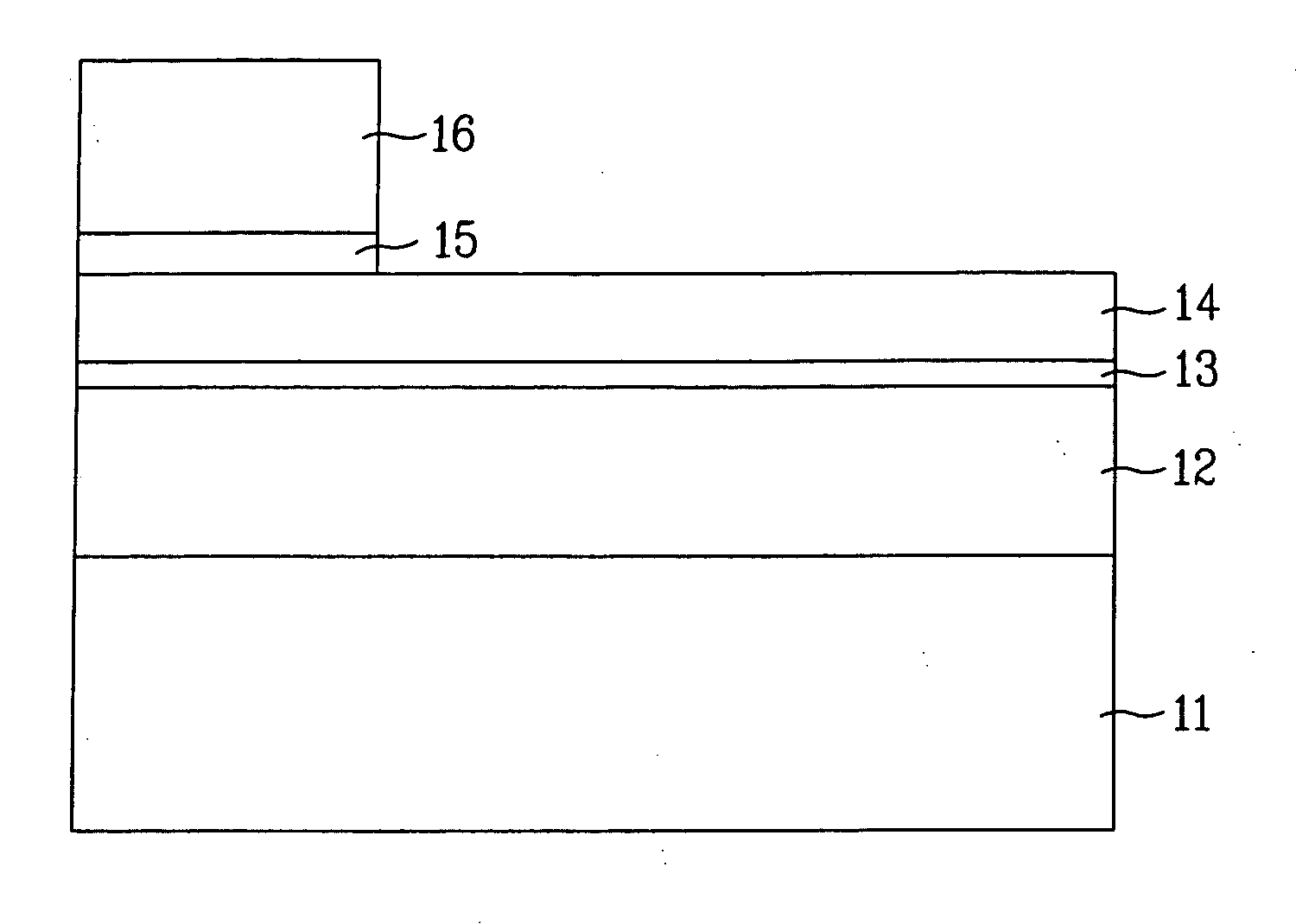
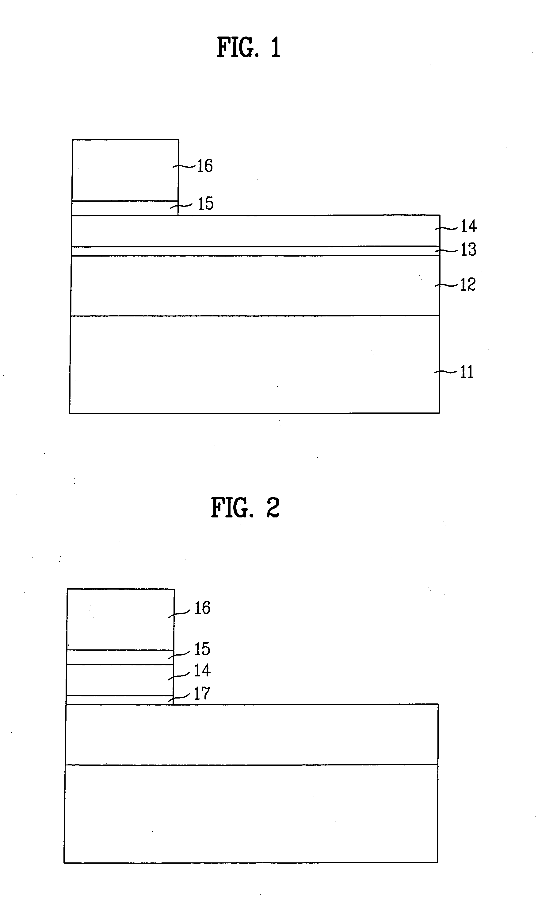
[0019]FIG. 1 and FIG. 2 illustrate cross sectional views showing a method of etching an upper metal layer of a capacitor in accordance with the present invention.

[0020]FIG. 1 shows a result material 16 formed on an upper nitride layer 15, which in turn is formed on an upper metal layer 14, lower nitride layer 13 (shown as 17 in FIG. 2), lower metal layer 12 and substrate 11.

[0021] Upper metal layer 11 is formed of Ti / TiN for example. The lower metal layer 12 is shown as one layer, although it could also be formed as several layers (e.g., Ti / TiN, Al or Cu, and Ti / TiN).

[0022]FIG. 1 shows a step of forming a pattern 16 (made of photoresist) on a substrate 11 having a predetermined device formed thereon. Th...


PUM

PropertyMeasurementUnit
pressureaaaaaaaaaa
structureaaaaaaaaaa
areaaaaaaaaaaa

Abstract

A method for etching an upper metal film of a capacitor, enables a safe etching of the upper metal film of a capacitor by exploiting an over-etch step. The method for etching the upper metal film of the capacitor includes the steps of forming a lower metal film, a lower nitride film, an upper metal film, and an upper nitride film on a substrate having a predetermined device formed thereon, and then forming a pattern thereover; etching the upper nitride film with CHF3, Ar and Cl2 using the pattern; over etching the upper metal film more than 50% with CHF3, Ar and N2 using the pattern; etching the upper metal film with CHF3, Ar and N2 using the pattern; and etching the lower nitride film with CHF3 and Ar using the pattern.

Description

BACKGROUND OF THE INVENTION [0001] 1. Field of the Invention [0002] The present invention relates to a method for etching an upper metal of a capacitor, and more particularly, to a method for forming an upper metal layer of a capacitor by over etching more than 50% in combination with using CHF3, Ar, and N2. [0003] 2. Discussion of the Related Art [0004] Recently, as a degree of device integration becomes higher, a cell area allocated for reading and recording an electric signal is gradually reduced. [0005] For example, in a case of 256 Mb DRAM, the cell area is 0.5 μm 2. In this case, an area allocated to a capacitor, as one of basic elements of the cell, should be less than 0.3 μm 2. [0006] According to such an improvement of integration of the semiconductor device, a method has been introduced for forming the capacitor with a dielectric film having a high electric constant, forming the dielectric film to be thin, or increasing an area of the capacitor, so as to secure high capaci...

Claims


Application Information

Patent Timeline
Patent Type & Authority Applications(United States)
IPC IPC(8): C23F4/00H01L21/02H01L21/3065H01L21/3213
CPCC23F4/00H01L28/60H01L21/32136H01L21/3065
Inventor YEOUN, JO BO
Owner DONGBU ELECTRONICS CO LTD
Learn More