
Semiconductor device

Inactive Publication Date: 2005-06-30
SEIKO EPSON CORP
View PDF2 Cites 3 Cited by
  • Summary
  • Abstract
  • Description
  • Claims
  • Application Information

AI Technical Summary

Benefits of technology

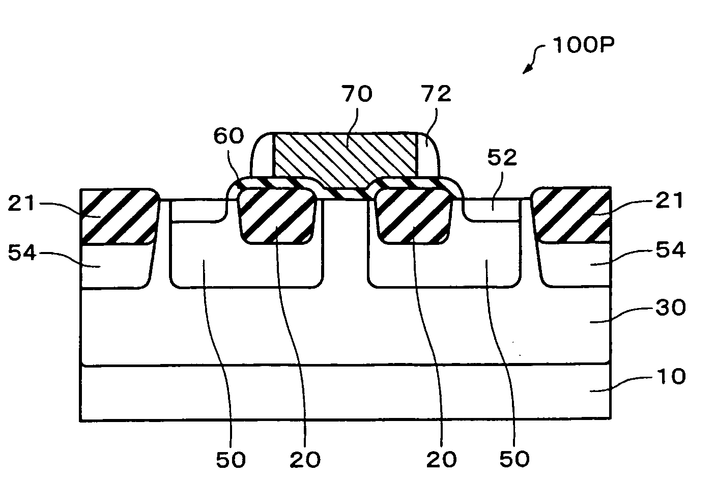
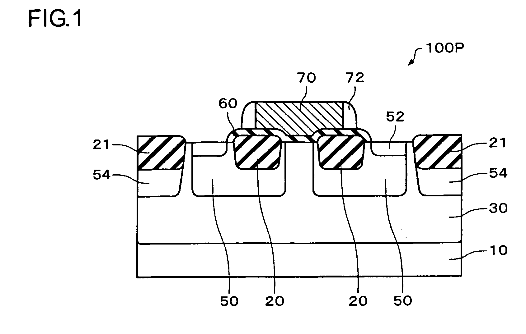
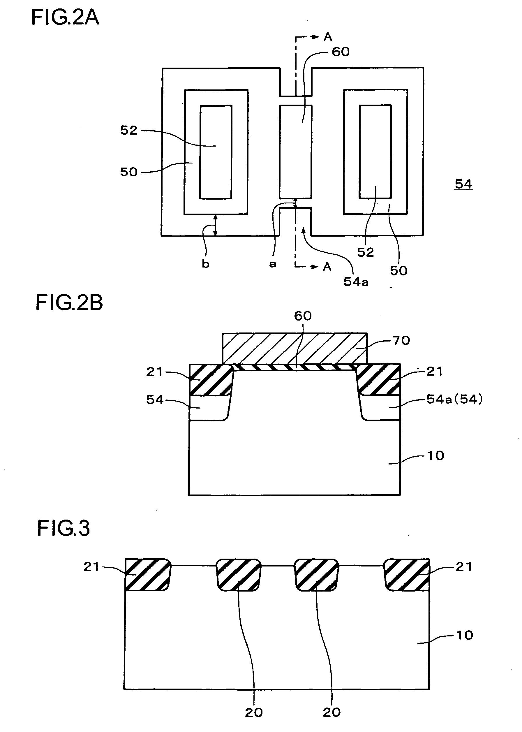
[0009] According to the present invention, the channel stopper region includes a protrusion so as to make the distance short between the gate insulation layer and the channel stopper region in a plan view. Namely, it includes a protrusion along the direction which makes the distance narrower between the channel region and the channel stopper region. This results in reducing a leak current. On the other hand, withstanding voltage can be assured in an area between offset region and the channel stopper region due to holding the desired distance. Namely, according to a semiconductor device of the present invention, both withstanding voltage and reducing a leak current can be improved as forming a partial protrusion so as to make only the distance narrower between the channel stopper region and the channel region. Further, a narrow area is formed so as to be partially protruded only in the region in which the distance to the channel stopper region is narrowed. Hence, there is no necessity of changing a semiconductor device as a whole. As the result, it can be provided a semiconductor device in which micro-miniaturization is realized in addition to the above advantage.

Problems solved by technology

However, enlarging the channel region comparing to the source / drain region 152 described above sometime faces insufficient micro-miniaturization of a transistor.

Method used


Image

  • Semiconductor device
  • Semiconductor device
  • Semiconductor device

Examples


Embodiment Construction

[0020] Embodiments of the invention will now be described with reference to FIGS. 1 and 2. FIG. 1 is a cross section schematically showing a semiconductor device of the embodiment. FIG. 2A is a plan view schematically showing the positional relationship between a source / drain region and a channel stopper region in the embodiment. FIG. 2B is a cross sectional view taken along the line A-A shown in FIG. 2A. In the embodiment, it will be explained an example in which P channel high voltage transistor 100P is formed on a semiconductor substrate 10. The example is for descriptive purpose and it can be surely applied to a semiconductor device of a hybrid structure including more than two different kinds of transistors.

[0021] According to a semiconductor device of the embodiment, as shown in FIG. 1, the P channel high voltage transistor 100P is formed in the region for forming a transistor which is partitioned by a element isolation insulation layer 21 fabricated in the semiconductor subs...


PUM


Abstract

A semiconductor device is provided including a gate insulation layer formed on a semiconductor substrate, a source and drain region, an offset region composed of a doped layer of which concentration is low comparing to that of the source region and drain region and surrounds the source region and drain region, and a channel stopper region formed on the outside of the offset region. The channel stopper region includes a protrusion toward the long side direction of the gate insulation layer such that the distance between the gate insulation layer and the channel stopper region is narrower than the distance between the offset region and the channel stopper region.

Description

RELATED APPLICATIONS [0001] This application claims priority to Japanese Patent Application No. 2003-429403 filed Dec. 25, 2003 which is hereby expressly incorporated by reference herein in its entirety. BACKGROUND [0002] 1. Technical Field [0003] The present invention relates to a semiconductor device including a high voltage transistor driven with high voltage. In particular, it relates a semiconductor device including a high voltage transistor of which characteristics and micro-miniaturization are improved. [0004] 2. Related Art [0005] A high voltage transistor driven with high voltage needs the sufficient distance between an offset region and a channel stopper region to assure the high voltage proof FIG. 10 shows one of the conventional high voltage transistors that is explained hereafter. FIG. 10 is a plan view schematically showing the positional relationship between an offset region 150 and a channel stopper region 154 in the conventional high voltage transistor. As shown in ...

Claims


Application Information

Patent Timeline
IPC IPC(8): H01L21/336H01L27/148H01L21/76H01L29/06H01L29/10H01L29/78
CPCH01L29/0649H01L29/66568H01L29/1033
Inventor AKIBA, TAKAHISATSUYUKI, MASAHIKOYOKOYAMA, KENJI
Owner SEIKO EPSON CORP
Learn More