
Exposure method and apparatus

a technology applied in the field of exposure method and apparatus, can solve the problems of lowering throughput, unable to find information between timings of the flatness of the wafer, and affecting the accuracy of focus detection of the exposure area, so as to achieve the effect of correcting focusing and not lowering throughpu

Inactive Publication Date: 2005-06-16
CANON KK
View PDF9 Cites 10 Cited by
  • Summary
  • Abstract
  • Description
  • Claims
  • Application Information

AI Technical Summary

Benefits of technology

[0014] Accordingly, it is an exemplified object of the present invention to provide an exposure method and apparatus for successfully correcting the focusing to the wafer surface's flatness without lowering the throughput.

Problems solved by technology

A wafer having the bad flatness has disadvantageous focus detection accuracy of the exposure area.
As a result, there is no information available between timings of the flatness of the wafer.
The finer measurement timing in the scan direction and the increased number of measurement points in the oblique light irradiating system would reduce an offset error, but might disadvantageously lower the throughput due to the deteriorated scan speed in exposure time, increase measurement time and cost together with the complicated apparatus structure, and grows likelihood of troubles.

Method used


Image

  • Exposure method and apparatus
  • Exposure method and apparatus
  • Exposure method and apparatus

Examples


Embodiment Construction

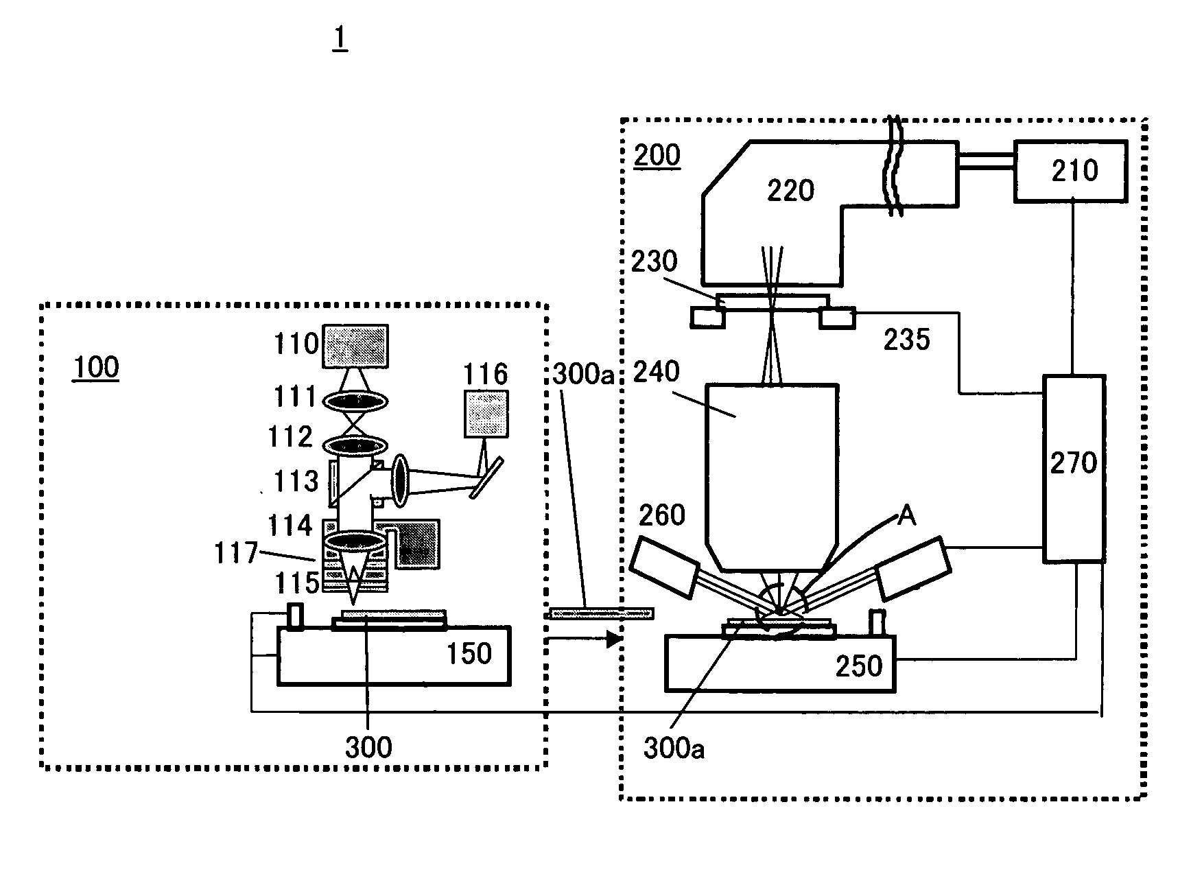
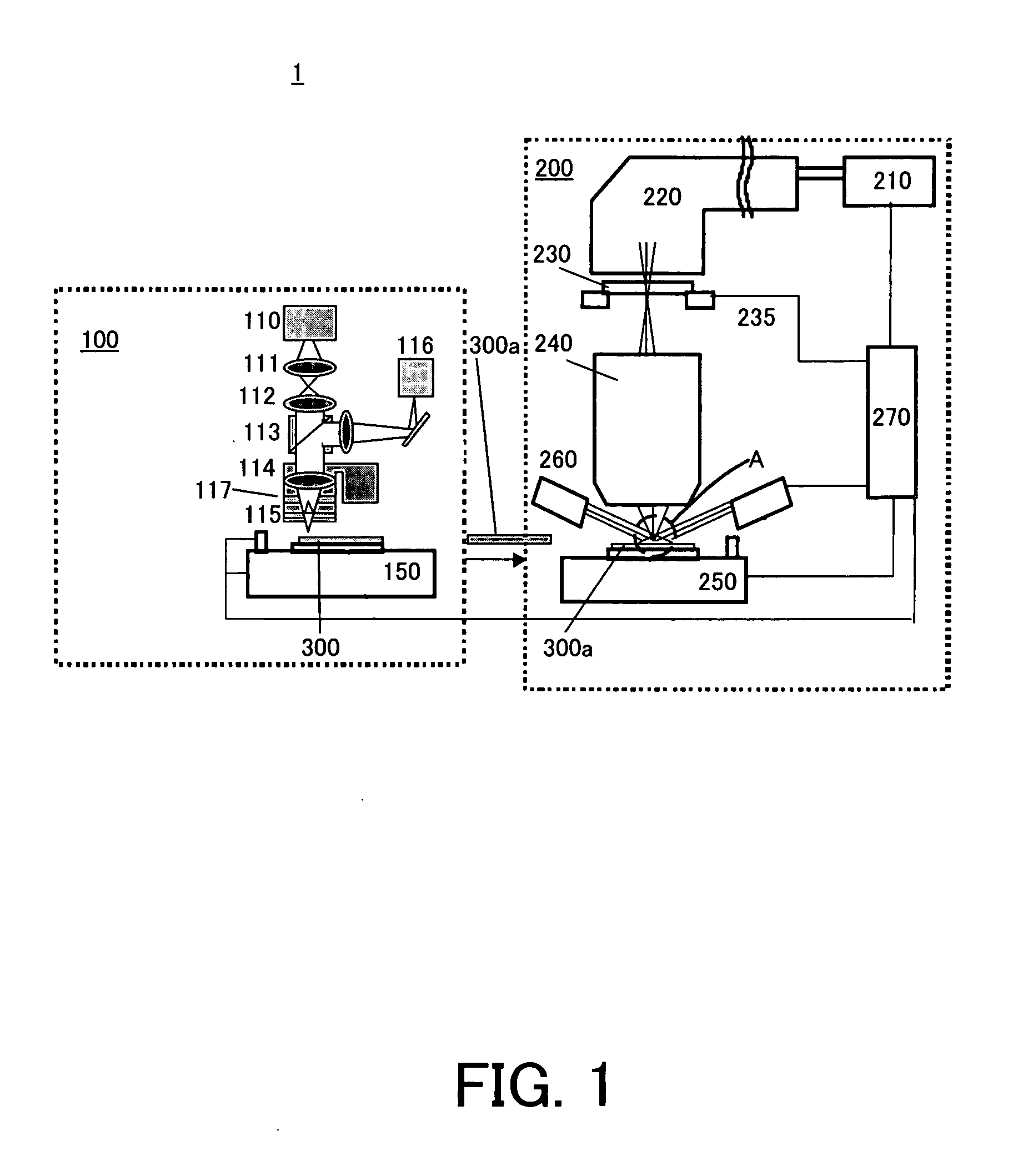
[0033] A description will now be given of an exposure apparatus and method of one embodiment according to the present invention with reference to the accompanying drawings. In each figure, the same element is designated by the same reference numeral, and a duplicate description thereof will be omitted. Here, FIG. 1 is a block diagram of a schematic structure of an exposure apparatus 1 according to one aspect of the present invention.

[0034] The exposure apparatus 1 includes, as shown in FIG. 1, a measuring station 100, and an exposure station 200, and serves as a projection exposure apparatus that exposes onto a wafer a circuit pattern on a reticle, for example, in a step-and-scan manner. Such an exposure apparatus is suitable for a sub-micron or quarter-micron lithography process.

[0035] A description will now be given of a measuring station 200 that measures the flatness of the plural shots on the wafer 300 prior to the semiconductor manufacture process. The measuring station 200 ...


PUM

PropertyMeasurementUnit
wavelengthaaaaaaaaaa

Abstract

An exposure method for exposing a pattern on a reticle onto plural shots on an object, includes the steps of measuring flatness information of each of the plural shots on the object, identifying a shot as a specific shot among the plural shots, the specific shot having flatness that is measured in the measuring step and outside a predetermined range, obtaining positional information by measuring plural measurement points on the object, the obtaining step obtaining more detailed positional information of the specific shot identified by the identifying step than that of a non-specific shot that is not the specific shot, and controlling at least one of a position and a tilt of the object using the positional information obtained by the obtaining step.

Description

BACKGROUND OF THE INVENTION [0001] The present invention relates generally to an exposure method and apparatus, and more particularly to an exposure method and apparatus used to expose various objects such as a single crystal substrate for a semiconductor wafer, a glass plate for a liquid crystal display (“LCD”), and the like. The present invention is suitable, for example, an exposure method and apparatus that utilizes a step and scan manner for exposure. [0002] Conventionally used projection exposure apparatuses use a projection optical system to project a circuit pattern on a mask (or a reticle) onto a wafer, etc. in manufacturing such devices as a semiconductor device, a LCD device and a thin-film magnetic head in the photolithography technology. [0003] The trend of the fine and high-density integrated circuits requires the projection exposure apparatus to expose a circuit pattern on the reticle onto a wafer with high resolving power. The minimum critical dimension transferable ...

Claims


Application Information

Patent Timeline
Patent Type & Authority Applications(United States)
IPC IPC(8): G03B27/52G03F7/20H01L21/027
CPCG03B27/52G03F9/7034G03F9/7011
Inventor INA, HIDEKI
Owner CANON KK
Learn More