Method of manufacturing liquid crystal display device and one drop fill apparatus used for the same
a technology drop filling device, which is applied in the direction of chemistry apparatus and processes, identification means, instruments, etc., can solve the problems of reducing the production efficiency affecting the product quality of the product, and reducing the defect rate of liquid crystal display device. , to achieve the effect of stable manufacturing process and reduced product defects
- Summary
- Abstract
- Description
- Claims
- Application Information
AI Technical Summary
Benefits of technology
Problems solved by technology
Method used
Image
Examples
first embodiment
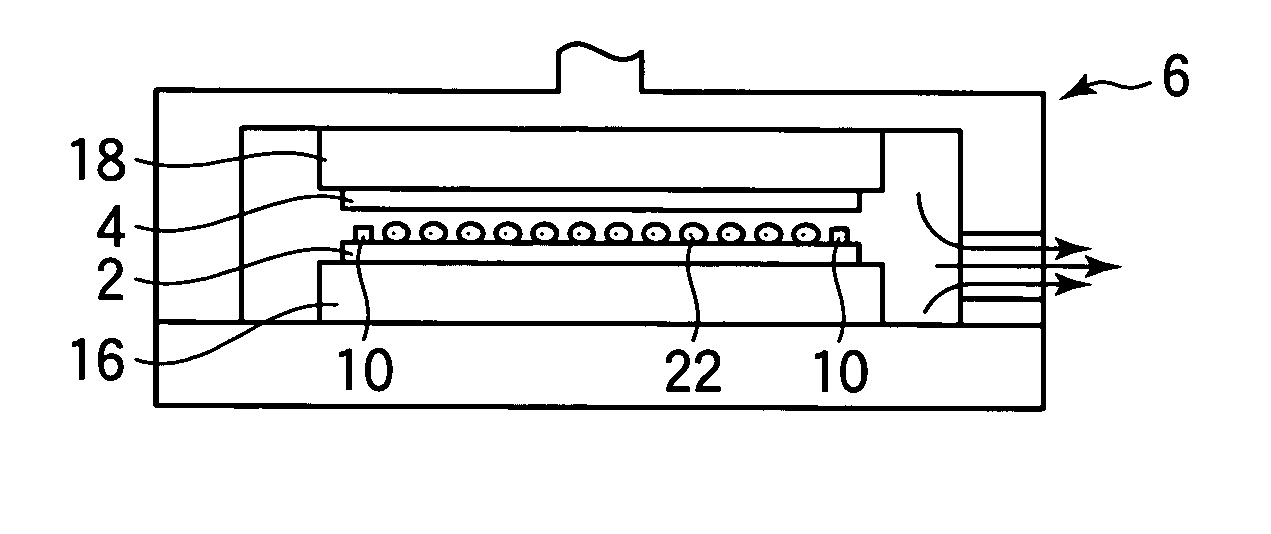
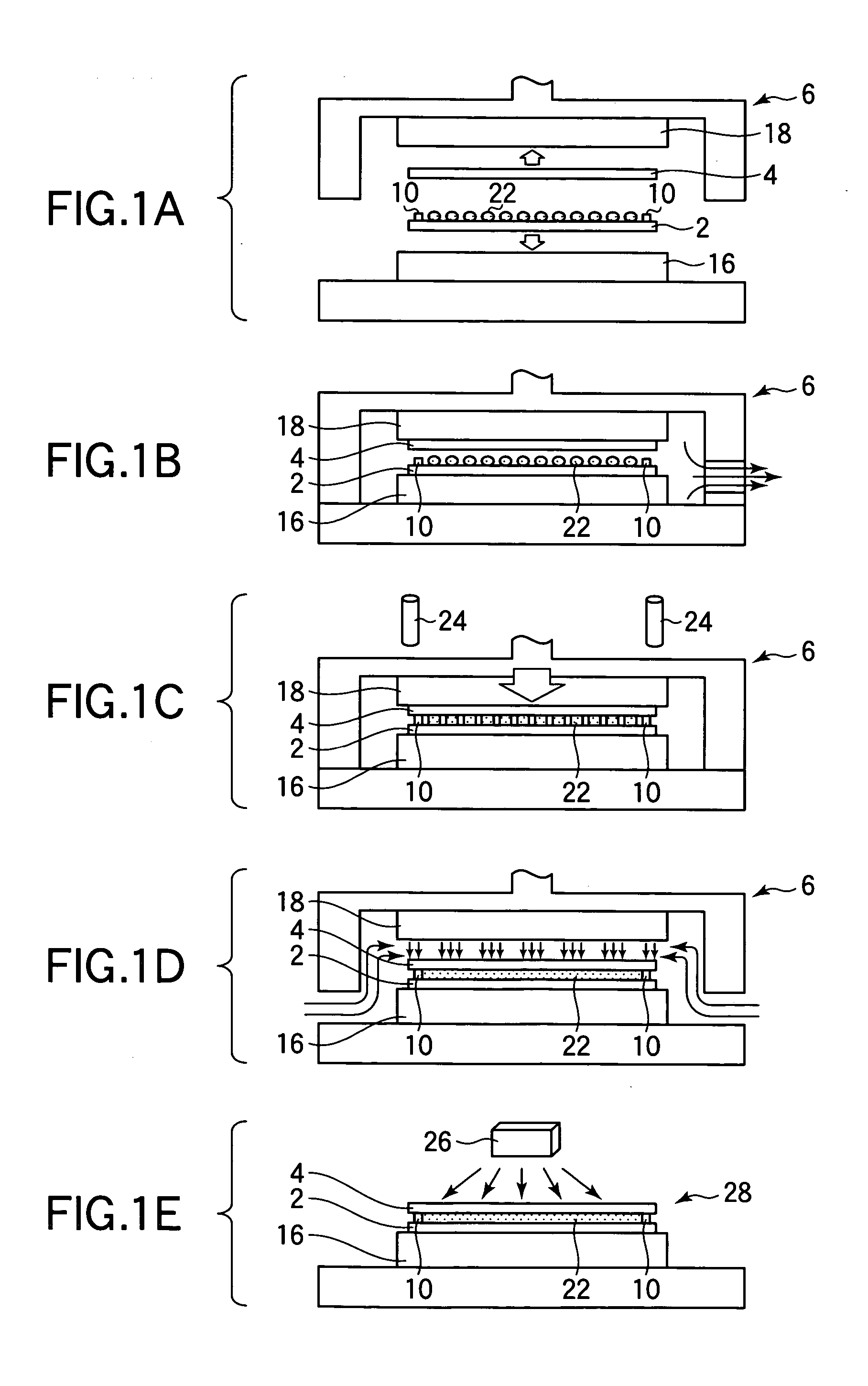
[0022] A method of manufacturing a liquid crystal display device using a one drop fill method and a one drop fill apparatus according to a first embodiment of this invention will now be described with reference to FIG. 1A to FIG. 6. A substrate laminating step and a liquid crystal injection step for a liquid crystal display device will be described with reference to FIGS. 1A to 1E. As shown in FIG. 1A, a seal material 10 made of, for example, a photosensitive hardening resin, is applied in a frame-shape, for example, on an outer peripheral part of a TFT substrate 2 of two substrates 2 and 4 on which an alignment films are formed. The seal material 10 is formed to a height of approximately 30±5 μm on the TFT substrate 2. On the CF substrate 4 arranged to face the TFT substrate 2, pillar spacers made of a resin are formed or spherical spacers are scattered and adhered.
[0023] Next, using a dispenser (not shown), a predetermined quantity of liquid crystal 22 is dropped at predetermined...
second embodiment
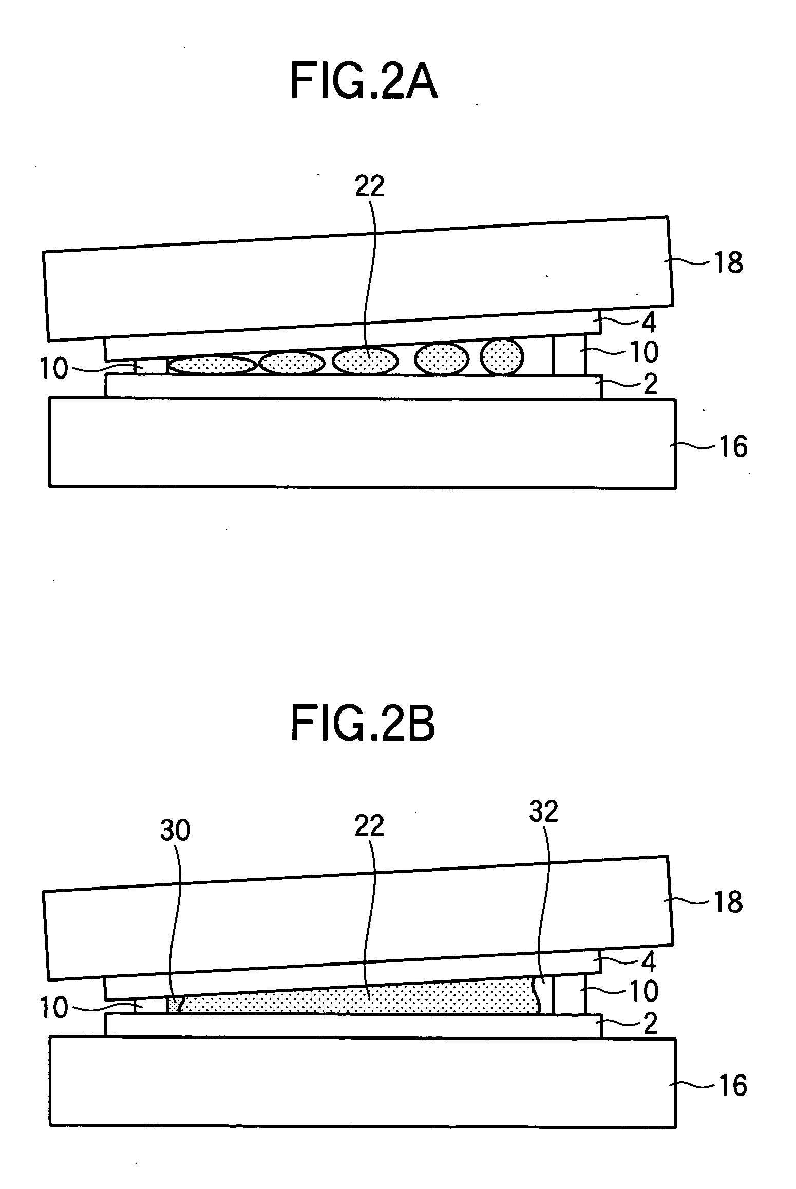
[0051] Now, a method of manufacturing a liquid crystal display device using a one drop fill method and a one drop fill apparatus used in the method according to a second embodiment of this invention will be described with reference to FIG. 7A to FIG. 9. FIGS. 7A and 7B are sectional views showing the spreading state of the liquid crystal 22 on the TFT substrate 2 and the CF substrate 4 with their substrate surfaces flexed and distorted. FIG. 7A is a sectional view showing a state where the liquid crystal 22 is spreading in the cell gap between the TFT substrate 2 and the CF substrate 4. FIG. 7B is a sectional view showing a state where the liquid crystal 22 is spread within the frame of the seal material 10. Constituent elements having the same effects and functions as the constituent elements in the method of manufacturing a liquid crystal display device and the one drop fill apparatus 60 used for the method of the first embodiment shown in FIG. 1A to FIG. 4 are denoted by the same...
third embodiment
[0061] A method of manufacturing a liquid crystal display device using a one drop fill method and a one drop fill apparatus used for the method according to a third embodiment of this invention will now be described with reference to FIG. 10A, FIG. 10B, FIG. 11A and FIG. 11B. While the one drop fill method is applied to each liquid crystal display panel 28 in the above-described first and second embodiments, this embodiment is characterized in that the one drop fill method is used on a multiple-panel substrate (mother substrate) for simultaneously manufacturing plural liquid crystal display panels 28. FIG. 10A is a sectional view showing a state where a mother substrate 66 for TFT substrate and a mother substrate 68 for CF substrate are set on a mother substrate lower plate 70 and a mother substrate upper plate 72, respectively. Since the mother substrate 66 for TFT substrate and the mother substrate 68 for CF substrate have a size large enough to provide, for example, four liquid c...
PUM
| Property | Measurement | Unit |
|---|---|---|
| Time | aaaaa | aaaaa |
| Pressure | aaaaa | aaaaa |
| Width | aaaaa | aaaaa |
Abstract
Description
Claims
Application Information
 - R&D Engineer
- R&D Manager
- IP Professional
- Industry Leading Data Capabilities
- Powerful AI technology
- Patent DNA Extraction
Browse by: Latest US Patents, China's latest patents, Technical Efficacy Thesaurus, Application Domain, Technology Topic, Popular Technical Reports.
© 2024 PatSnap. All rights reserved.Legal|Privacy policy|Modern Slavery Act Transparency Statement|Sitemap|About US| Contact US: help@patsnap.com


