
Method of forming trench isolation in the fabrication of integrated circuitry

a technology of integrated circuitry and trench isolation, which is applied in the direction of coatings, chemical vapor deposition coatings, metallic material coating processes, etc., can solve the problem of greater shrinkage in the horizontal dimension than in the vertical dimension

Inactive Publication Date: 2005-06-09
MICRON TECH INC
View PDF77 Cites 130 Cited by
  • Summary
  • Abstract
  • Description
  • Claims
  • Application Information

AI Technical Summary

Benefits of technology

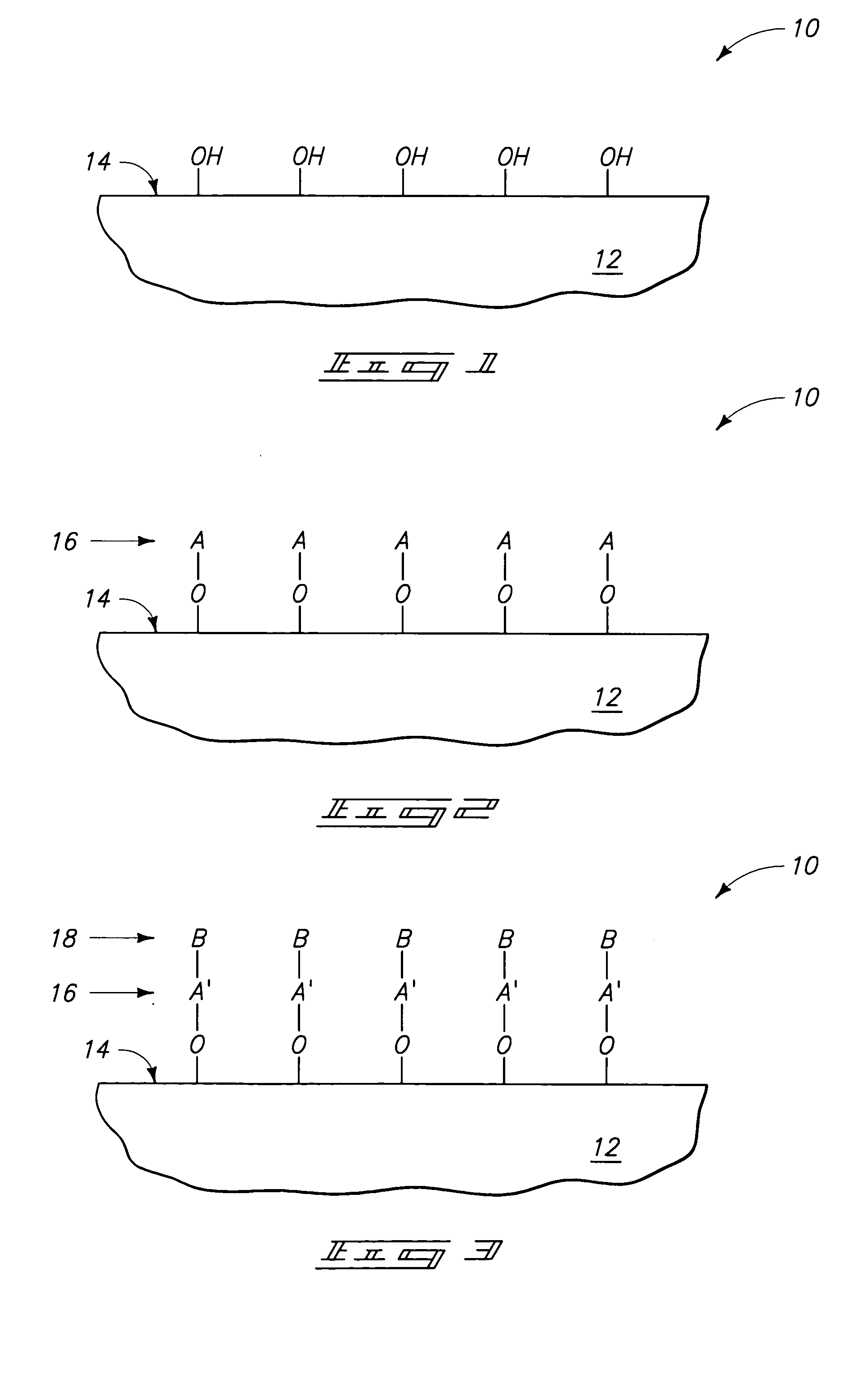
This patent describes methods for making phosphorus doped silicon dioxide layers and for creating trench isolation in the fabrication of integrated circuitry. The methods involve depositing layers of phosphorus doped silicon dioxide onto a substrate using specific vapor phase reactants. The first reactant is a compound called PO(OR)3, where R is a hydrocarbyl group, and the second reactant is a compound called Si(OR)3OH, where R is also a hydrocarbyl group. The process involves chemisorbing a first species onto the substrate surface and then contacting it with a second species to form a monolayer of silicon and oxygen. This process is repeated to create a layer of phosphorus doped silicon dioxide on the substrate. The technical effect of this patent is to provide new methods for making phosphorus doped silicon dioxide layers that can be used in the fabrication of integrated circuitry.

Problems solved by technology

As semiconductor devices continue to shrink geometrically, such has had a tendency to result in greater shrinkage in the horizontal dimension than in the vertical dimension.

Method used


Image

  • Method of forming trench isolation in the fabrication of integrated circuitry
  • Method of forming trench isolation in the fabrication of integrated circuitry
  • Method of forming trench isolation in the fabrication of integrated circuitry

Examples


Embodiment Construction

[0015] This disclosure of the invention is submitted in furtherance of the constitutional purposes of the U.S. Patent Laws “to promote the progress of science and useful arts” (Article 1, Section 8).

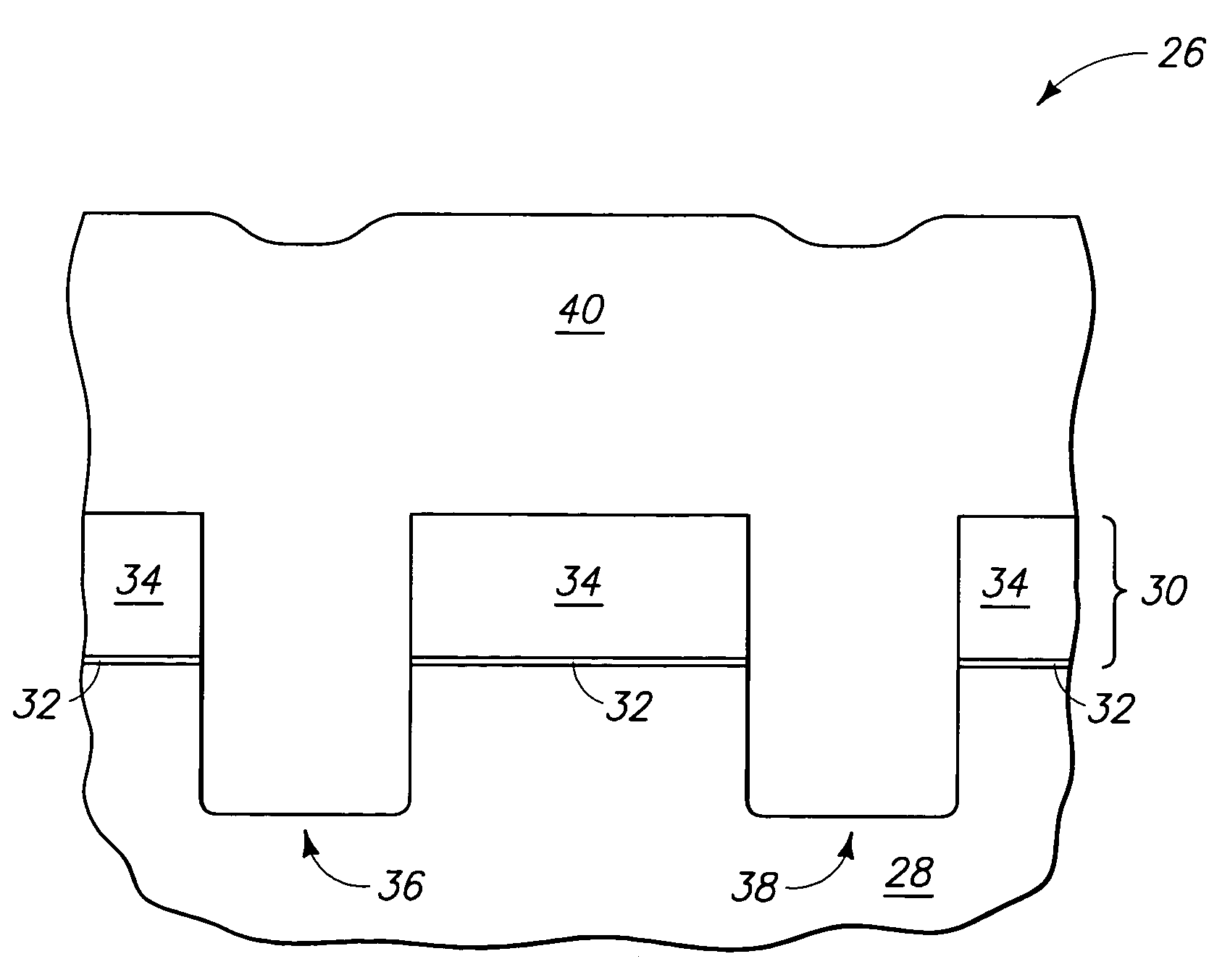
[0016] In one implementation, a method of forming a phosphorus doped silicon dioxide comprising layer includes positioning a substrate to be deposited upon within a deposition chamber. First and second vapor phase reactants are introduced in alternate and temporally separated pulses to the substrate within the chamber in a plurality of deposition cycles under conditions effective to deposit a phosphorus doped silicon dioxide comprising layer on the substrate. One of the first and second vapor phase reactants is PO(OR)3, where R is hydrocarbyl. An other of the first and second vapor phase reactants is Si(OR)3OH, where R is hydrocarbyl. Such might be conducted by atomic layer deposition (ALD) methods (for example including chemisorbing and contacting methods), by chemical vapor deposition...


PUM

PropertyMeasurementUnit
temperatureaaaaaaaaaa
thicknessaaaaaaaaaa

Abstract

This invention includes methods of forming a phosphorus doped silicon dioxide comprising layers, and methods of forming trench isolation in the fabrication of integrated circuitry. In one implementation, a method of forming a phosphorus doped silicon dioxide comprising layer includes positioning a substrate within a deposition chamber. First and second vapor phase reactants are introduced in alternate and temporally separated pulses to the substrate within the chamber in a plurality of deposition cycles under conditions effective to deposit a phosphorus doped silicon dioxide comprising layer on the substrate. One of the first and second vapor phase reactants is PO(OR)3 where R is hydrocarbyl, and an other of the first and second vapor phase reactants is Si(OR)3OH where R is hydrocarbyl.

Description

TECHNICAL FIELD [0001] This invention relates to methods of forming phosphorus doped silicon dioxide comprising layers, and to methods of forming trench isolation in the fabrication of integrated circuitry. BACKGROUND OF THE INVENTION [0002] One commonly used material in the fabrication of integrated circuitry is silicon dioxide. Such might be utilized as essentially 100% pure, or in combination with other materials, including property-modifying dopants. Accordingly, silicon dioxide might be utilized as a mixture with other materials in forming a layer or layers and may or may not constitute a majority of the given layer. Exemplary materials are borophosphosilicate glass (BPSG), phosphosilicate glass (PSG), and borosilicate glass (BSG). Typically, such materials have anywhere from 1% to 4% atomic concentration of each of boron and / or phosphorus atoms, although atomic percent concentrations in excess of 5% have also been used. [0003] As semiconductor devices continue to shrink geomet...

Claims


Application Information

Patent Timeline
Patent Type & Authority Applications(United States)
IPC IPC(8): C23C16/04C23C16/40C23C16/44C23C16/455H01L21/316H01L21/762
CPCC23C16/045C23C16/401C23C16/402C23C16/45531H01L21/76227H01L21/02216H01L21/02271H01L21/0228H01L21/31625H01L21/02129H01L21/02164H01L21/02274C23C16/40H01L21/67207
Inventor VAARTSTRA, BRIAN A.
Owner MICRON TECH INC
Learn More