
Semiconductor module with scalable construction

a technology of semiconductor modules and semiconductor devices, applied in semiconductor devices, semiconductor/solid-state device details, electrical apparatus, etc., can solve problems such as disadvantages of automated production, and achieve the effect of easy and convenient production and easy integration

Inactive Publication Date: 2005-02-17
SEMIKRON ELECTRONICS GMBH & CO KG
View PDF1 Cites 0 Cited by
  • Summary
  • Abstract
  • Description
  • Claims
  • Application Information

AI Technical Summary

Benefits of technology

[0007] It is therefore an object of the present invention to present a power semiconductor module which is scalable in a simple way, so that power semiconductor modules of different power levels can be constructed with many identical components.
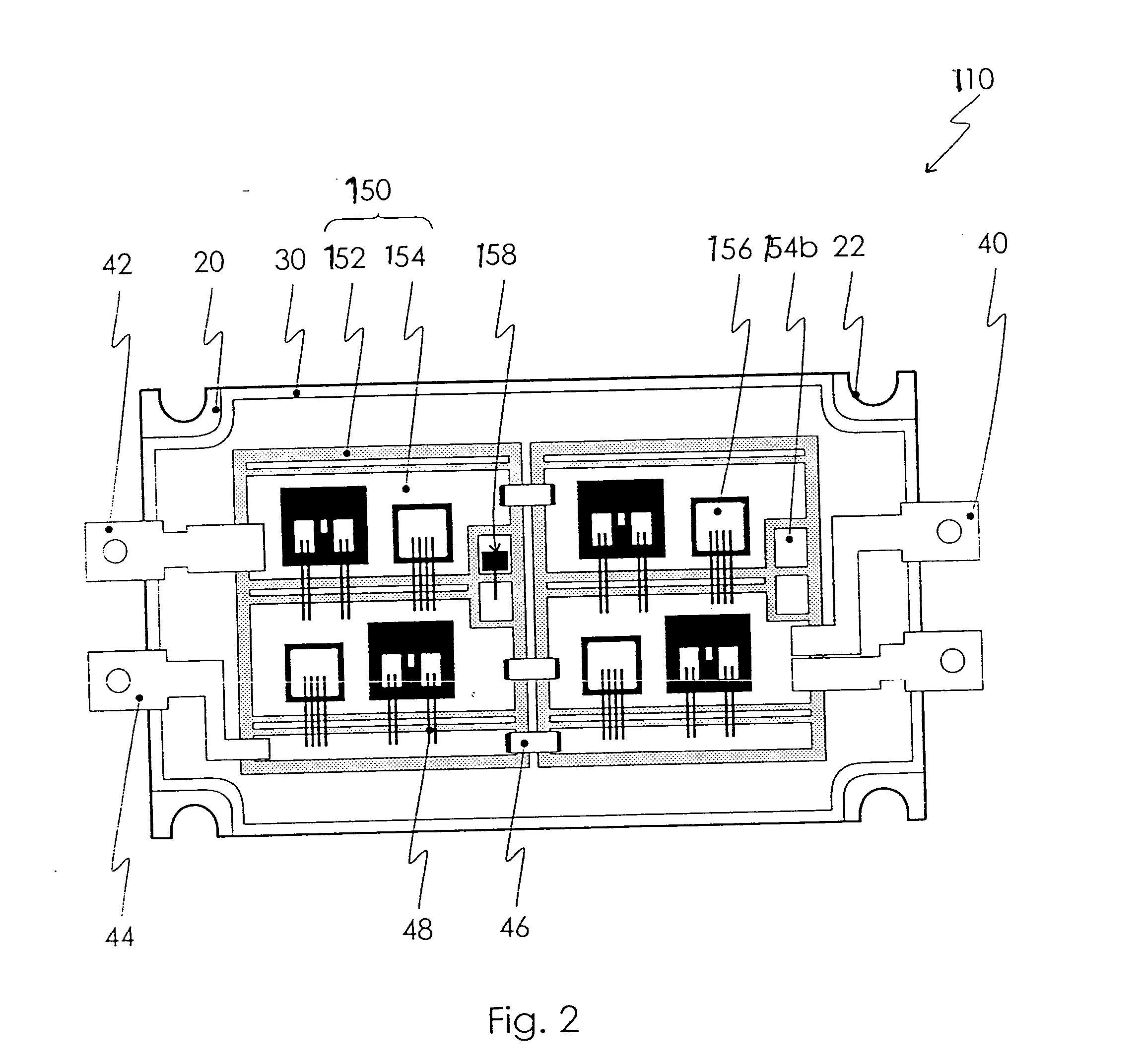
[0010] An advantage of this embodiment of the inventive power semiconductor module is that because of the completely identical substrates and the assembly with power semiconductor components, the module may be easily and conveniently produced, since for different power classes, only the number of substrates disposed in the power semiconductor module varies. Additional functionalities such as sensor system components can also be integrated easily, since the conductor tracks required for them are identically provided on each substrate. Thus, inside the power semiconductor module, the only difference is the assemblage of components, but not the type or shape of the substrates within the module. The terminal faces for connecting elements for the internal and external connection of the load and auxiliary terminals are thus likewise identical on all the substrates.

Problems solved by technology

This is disadvantageous to automated production, since for both different power classes and different voltage classes, different substrates are employed.

Method used


Image

  • Semiconductor module with scalable construction
  • Semiconductor module with scalable construction
  • Semiconductor module with scalable construction

Examples


Embodiment Construction

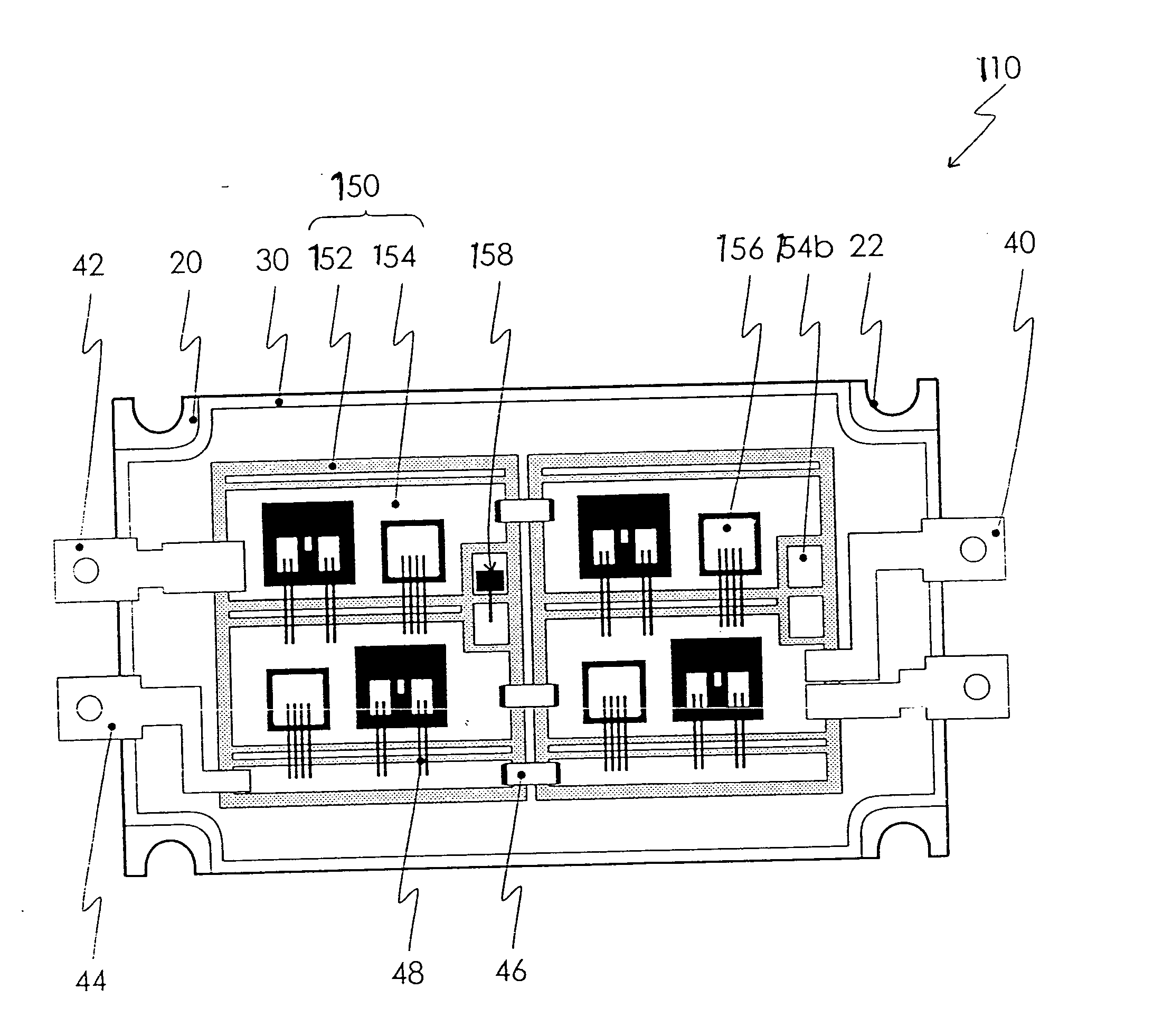
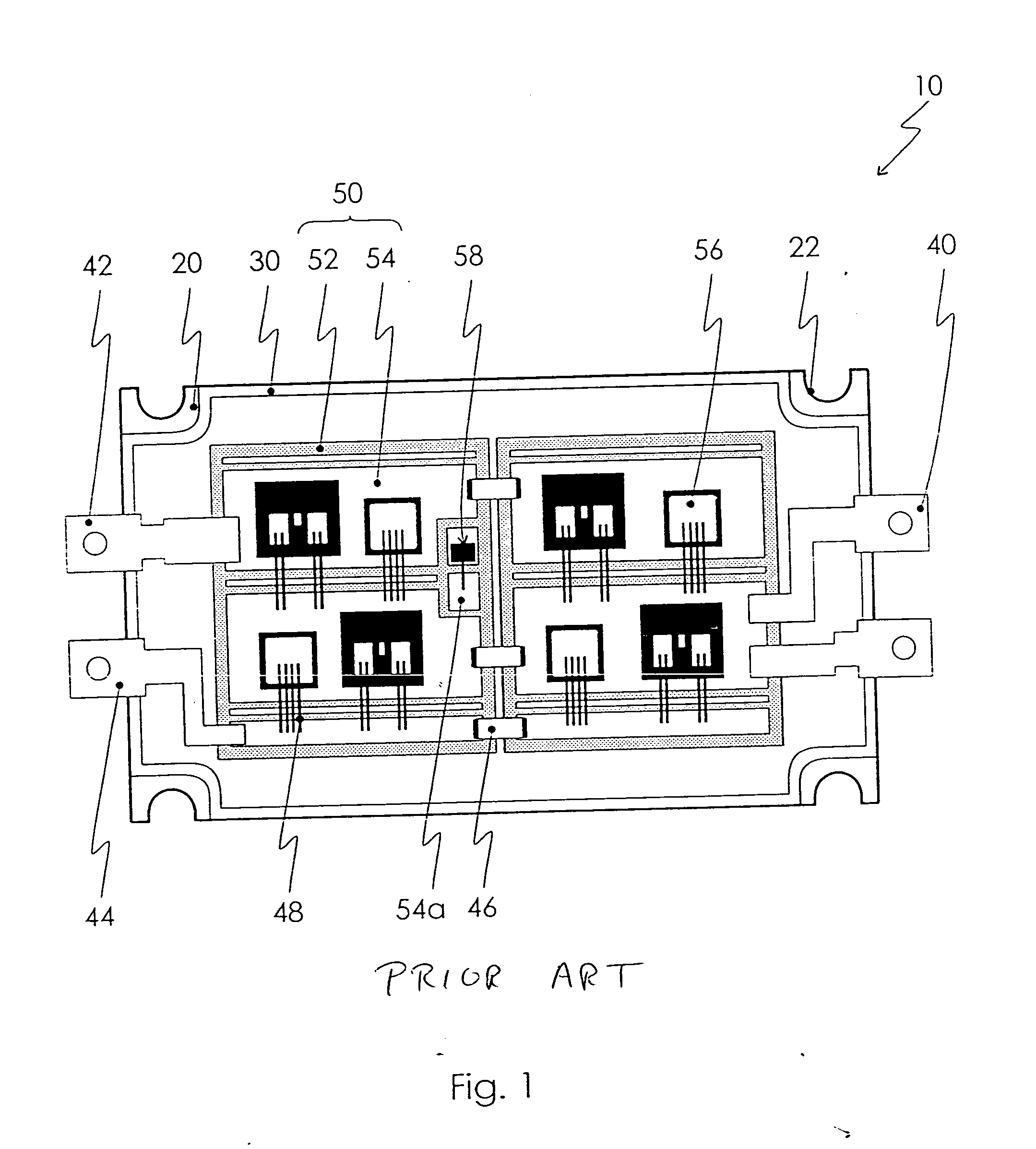
[0017]FIG. 1 shows a power semiconductor module of the prior art in plan view. A power semiconductor module 10 is shown, comprising a base plate 20, for mounting on a heat sink. For that purpose, this base plate 20 has one recess 22 in the vicinity of each of its corners. The module further comprises a framelike housing 30 as well as two electrically insulating substrates 50. Each substrate in turn comprises an insulating body 52, with a plurality of metal connecting tracks 54 insulated from one another and located on its first main face remote from the base plate 20. On its second main face, toward the base plate, the substrate has a two-dimensional metallization of the same type as the connecting tracks of the first main face. Power semiconductor components 56, and a sensor system component 58 are disposed on connecting tracks 54, and connected thereto by appropriate circuitry using wire bond connections 48. For establishing electrical contact with the exterior of housing 30, modu...


PUM


Abstract

A power semiconductor module with a scalable construction, having a base plate or intended for direct mounting on a heat sink. The module has a framelike housing, a cover, terminal elements, extending to the outside of the housing for load contacts and auxiliary contacts. The module having at least two electrically insulating substrates disposed inside the housing, which in turn each comprise one insulating body and a plurality of metal conducting tracks, located on the first main face of the insulating body, which first main face is remote from the base plate or the heat sink. The metal connecting tracks are electrically insulated from one another, and power semiconductor components are located on and electrically connected to these connecting tracks. The substrates (50) are identical, and electrically connected to one another, and have the same type and number of power semiconductor components disposed thereon.

Description

BACKGROUND OF THE INVENTION [0001] 1. Field of the Invention [0002] The invention is directed to a power semiconductor module, and, more particularly, to a power semiconductor module with a scalable construction. [0003] 2. Description of the Related Art [0004] Power semiconductor modules that are the point of departure for the present invention are known for instance from German Patent Disclosure DE 103 16 355. Such power semiconductor modules have defined voltage and power classes. As examples, the voltage classes of 600V, 1200V and 1700V are known. In the same way, various power classes are known. To enable covering a broad range of uses, power semiconductor modules corresponding to these classes are thus offered. To make it possible to assure rational production, given the many types involved, power semiconductor modules are offered in an identical external shape with identical terminal elements for different classes, for both voltage and power classes. Depending on the classes i...

Claims


Application Information

Patent Timeline
Patent Type & Authority Applications(United States)
IPC IPC(8): H01L23/34H01L25/07H01L25/18
CPCH01L23/34H01L25/072H01L2224/48227H01L2224/49111H01L2224/49175H01L2924/00H01L2224/0603H01L2224/49113
Inventor MANZ, YVONNESTEGER, JURGENSTOCKMEIER, THOMAS
Owner SEMIKRON ELECTRONICS GMBH & CO KG
Learn More