
Semiconductor device and method for fabricating the same

a technology of semiconductor devices and semiconductors, applied in semiconductor devices, semiconductor/solid-state device details, electrical apparatus, etc., can solve problems such as the reduction of production efficiency, and achieve the effect of increasing inductan

Active Publication Date: 2004-12-02
LAPIS SEMICON CO LTD
View PDF10 Cites 20 Cited by
  • Summary
  • Abstract
  • Description
  • Claims
  • Application Information

AI Technical Summary

Benefits of technology

[0013] Accordingly, an object of the present invention is to provide a semiconductor device in which an increase in inductance can be realized without increasing further the area conventionally occupied by the coil.
[0018] The inductance of the coil when an electric current flows is proportional to the magnetic permeability around the coil. Therefore, according to this construction, it becomes possible to increase the inductance of the coil because the magnetic body is provided in the position surrounded by the coil.
[0019] Furthermore, comparing the case in which a magnetic body is provided, with the case in which an inductance of the same degree is to be obtained without providing such a magnetic body, the area occupied by the coil can be reduced, and enlargement of the semiconductor device can be restrained.

Problems solved by technology

As a result, because enlargement of the semiconductor chip becomes unavoidable, there is the concern that a reduction in the number of semiconductor chips formed from a single wafer leads to a decrease in production efficiency.

Method used


Image

  • Semiconductor device and method for fabricating the same
  • Semiconductor device and method for fabricating the same
  • Semiconductor device and method for fabricating the same

Examples


first embodiment

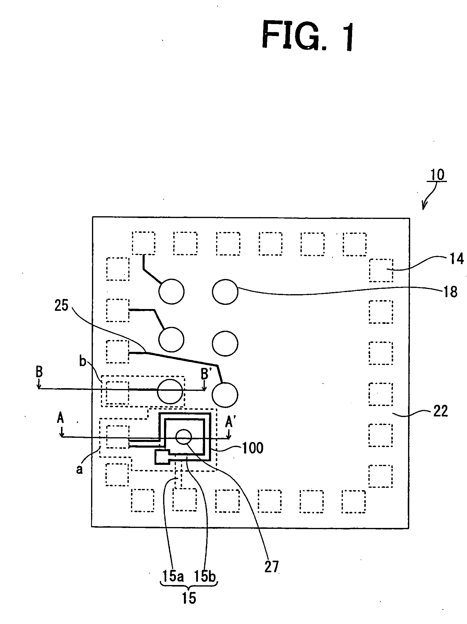
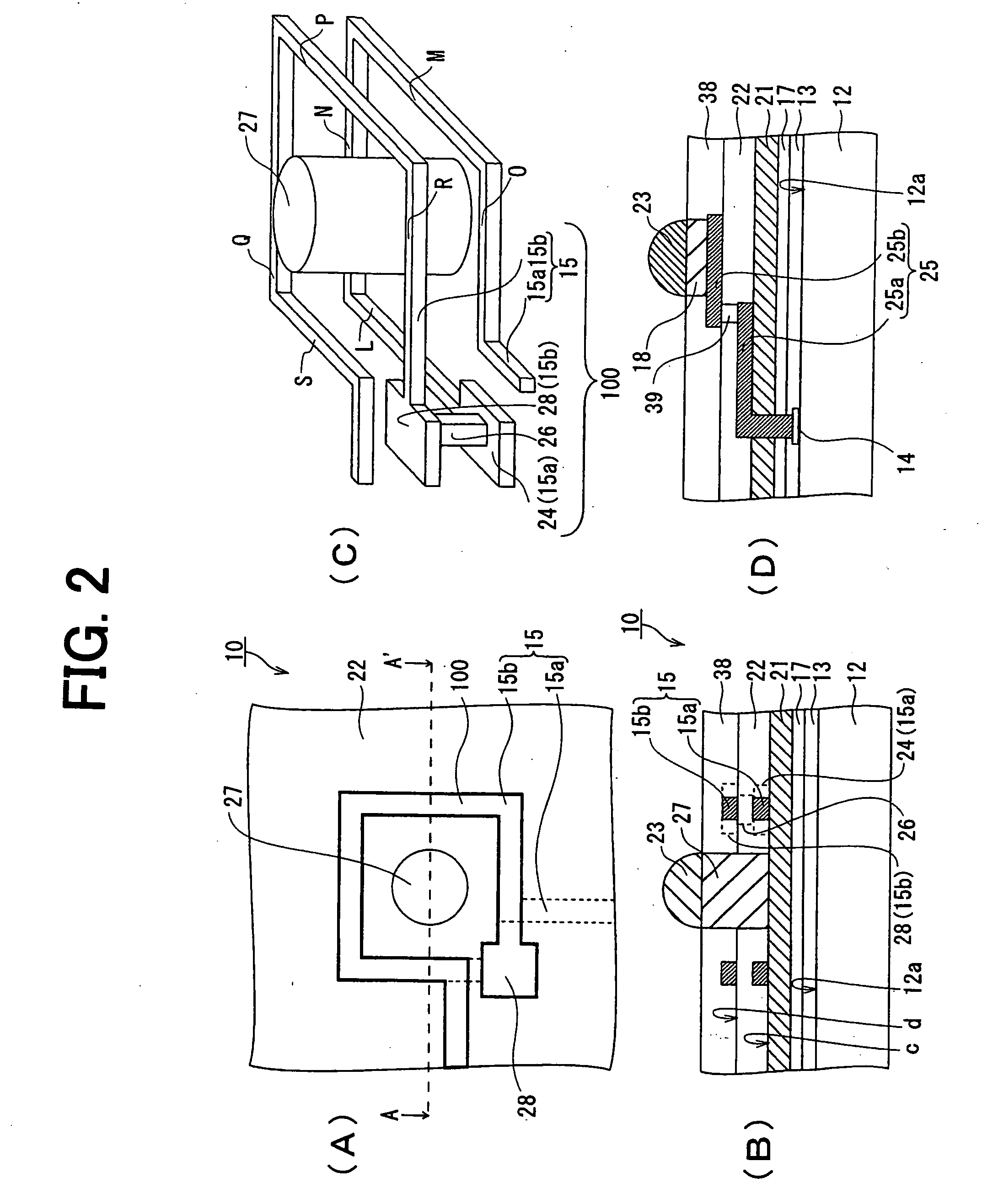
[0054] A semiconductor device according to the present invention is described with reference to FIG. 1 through FIG. 4. FIG. 1 is a schematic plan view omitting some components of a WCSP 10 which is the semiconductor device of this embodiment. In particular this is a diagram that shows the outline of each of the components drawn with solid lines, in order to show clearly the form and positional relationship of each components such as an electrode pad, a conductive part, a post part, a wiring layer and a pseudo-post part, and so on, on the semiconductor chip. Furthermore, FIG. 2(A) is a diagram schematically showing an enlargement of a first area shown in the plan view of FIG. 1 surrounded by a broken line "a", with an external terminal and a sealing layer omitted. Also, FIG. 2(B) is a simplified cross-sectional view showing an example of a component part corresponding to the section (specifically cross-section) obtained by cutting FIG. 1(A) along the broken line part A-A'. Moreover, ...

second embodiment

[0085] A semiconductor device according to the present invention is described with reference to FIG. 5 and FIG. 6. FIG. 5(A) and (B) are a simplified plan view, and an A-A' cross sectional view corresponding to FIG. 2(A) and (B) respectively, and FIG. 6(A) and (B) are production process diagrams which focus on and describe the part corresponding to FIG. 5. (B)

[0086] In the first embodiment mentioned above the external terminal 23 is provided on the end surface of the pseudo-post part 27. However the second embodiment differs from the first embodiment principally in that the end surface of the pseudo-post part does not have an external terminal and is covered by the sealing layer 38. In the second embodiment, the pseudo-post part without an external terminal provided is described as a magnetic core part 32. Also, the same components previously described in the first embodiment are shown with the same reference symbols, and their descriptions may be omitted (the same applies to each o...

third embodiment

[0099] A semiconductor device according to the present invention is described with reference to FIG. 7, through FIG. 9. FIG. 7(A) and (B) are a simplified plan view and a cross sectional view A-A' of the same type as (A) and (B) in FIG. 2. FIG. 8(A) through (C) are production process diagrams describing particularly the part corresponding to (B) in FIG. 7. FIG. 9(A) and (B) are production diagrams which follow FIG. 8(C). In FIG. 7(A), the external terminal is omitted. Moreover, each of the production process diagrams are sectional views on the cut face.

[0100] The main point of difference between this embodiment and the first embodiment is that the entire coil 100 which functions as a coil is embedded in the pseudo-post part 34 which is made from insulating material.

[0101] As shown in FIG. 7(A) and (B), on the second insulating layer 21 of a WCSP 55 in this embodiment, is formed the pseudo-post part 34 with the coil 100 substantially embedded therein except for a part on the side whi...


PUM

PropertyMeasurementUnit
Fractionaaaaaaaaaa
Thicknessaaaaaaaaaa
Electrical inductanceaaaaaaaaaa

Abstract

In a semiconductor device having a WCSP type construction package, to increase inductance without increasing further an area conventionally occupied by a coil. A pseudo-post part 27 comprising a magnetic body is extended in a direction perpendicular to a main surface 12a of a semiconductor chip 12, on a second insulating layer 21 of a WCSP 10. A first conductive part 15a and a second conductive part 15b constructed as square frames are respectively provided so as to surround the pseudo-post part, on respective top surfaces of a second insulation layer and a third insulating layer 22 which are separated parallel to each other, in an extension direction of the pseudo-post part. A coil 100 being a substantially spiral shape conductive path is formed from, the first conductive part, the second conductive part, and a connection part 26 which electrically connects the one ends of the first and second conductive parts.

Description

[0001] This application claims the priority of Application No. 2003-148430, filed May 26, 2003 in Japan, the subject matter of which is incorporated herein by reference.[0002] The present invention relates to a semiconductor device having a WCSP type packaging construction.[0003] Recently CSPs (Chip Size Packages), which are semiconductor devices packaged with effectively the same outer dimensions as those of semiconductor chips, have been proposed following a demand for high integration and miniaturization of semiconductor devices used in electronic equipment.[0004] Among such CSPs, WCSPs (Waferlevel CSPs) which are CSPs that are divided into pieces by dicing after the process of forming the external terminals has been completed while still in wafer form, are focused on with a view to reducing production costs (for example, see patent document 1).[0005] WCSPs have a construction having electrodes and external terminals on a semiconductor chip electronically connected to each other ...

Claims


Application Information

Patent Timeline
IPC IPC(8): H01L21/3205H01L23/52H01L21/822H01L23/12H01L23/31H01L23/522H01L27/04
CPCH01L23/3114H01L23/5227Y10T29/49073H01L2924/0002H01L2924/00
Inventor ANZAI, NORITAKATERUI, MAKOTO
Owner LAPIS SEMICON CO LTD
Learn More