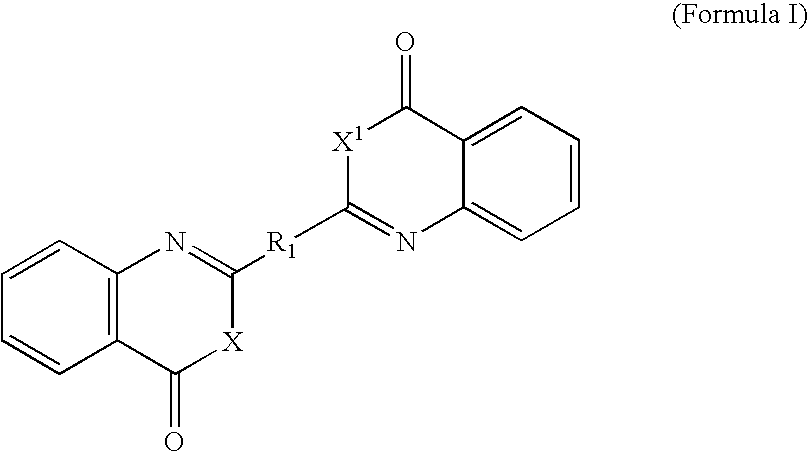
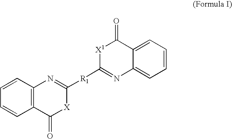
Benzoxazinone and quinazolinone derivatives
a technology of quinazolinone and benzoxazinone, which is applied in the direction of discharge tube luminescnet screen, organic semiconductor device, natural mineral layered product, etc., can solve the problems of low blue light emission performance of blue light emitting device, inability to achieve desirable emission colors, and inability to meet the requirements of the device in which the compound is incorporated
- Summary
- Abstract
- Description
- Claims
- Application Information
AI Technical Summary
Problems solved by technology
Method used
Image
Examples
example 1
[0083] In this example, a glass substrate with indium-tin-oxide (ITO) film having a thickness of 1500 .ANG. was placed into a rotational substrate holder inside a vacuum deposition chamber with the ITO layer facing a plurality of deposition boats containing materials to be deposited. A 400 .ANG. film of TPD was deposited through a first shadow mask having a square window overlapping the OLED pixel areas onto the ITO anode layer at a rate of 1-2 .ANG. / s to form a hole transport layer (HTL). Thereafter, a 300 .ANG. emitting layer (EML) was deposited via co-deposition of a dopant 2,2'-(1,4-phenylene)bis-4H-3,1-benzoxazin-4-one (1,3 PBBO) and a host compound, carbazole biphenyl (CBP), by means of thermal vapor deposition, through the same shadow mask. To achieve a 2.3% doping level, the deposition rate was maintained at about 0.05 .ANG. / s for the dopant and at about 2.4 .ANG. / s for the host during the course of deposition. For the former, control over such a low rate is usually difficul...
example 2
[0085] A series of OLEDs were fabricated in this example, where similarly to Example 1, glass substrates with indium-tin-oxide (ITO) film having a thickness of 1500 .ANG. were placed into a rotational substrate holder inside a vacuum deposition chamber with the ITO layer facing a plurality of deposition boats containing materials to be deposited. A 400 .ANG. film of TPD was deposited through a first shadow mask having a rectangular window overlapping the OLED pixel areas onto the ITO anode layer at a rate of 1-2 .ANG. / s to form a hole transport layer (HTL). Thereafter, about a 300 to 400 .ANG. thick emitting layer (EML) was deposited via co-deposition of a dopant 2,2'-(1,3-phenylene)bis-4H-3,1-be-nzoxazin-4-one (1,3 PBBO) and a host compound, carbazole biphenyl (CBP), by means of thermal vapor deposition, through the same shadow mask. During the course of deposition, the evaporation rates are maintained in such way that various doping concentrations ranging from 0 wt. % to 2.3 wt. %...
example 3
[0087] This example is similar to most of the fabrication steps to that of Example 1, except a 400 .ANG. EML was deposited via co-deposition of a dopant, 2,2'-(1,4-phenylene)bis-4H-3,1-benzoxazin-4-one (1,4 PPO), and a CBP host. The deposition rate was maintained at about 0.04 .ANG. / s. for the dopant and at about 1.0 .ANG. / s for the host during the course of deposition to achieve a 3.9 wt. % doping level. As in Example 1, to improve the control, the sensitivity of a thickness monitor was set to a factor of ten times higher than usual, and thus the real-time monitoring thickness was 0.4 .ANG. / s, while the real deposition rate was still 0.04 .ANG. / s. Maintaining the deposition rate at the aforementioned ratio provides a weight ratio of 3.9:96.1 for dopant and host, respectively. A 100 .ANG. hole blocking layer (HBL) of BCP was further deposited through the same shadow mask, followed by deposition of a 350 .ANG. electron transport layer (ETL) of Alq.sub.3. Thereafter, the first shadow ...
PUM
| Property | Measurement | Unit |
|---|---|---|
| Nanoscale particle size | aaaaa | aaaaa |
| Wavelength | aaaaa | aaaaa |
| Composition | aaaaa | aaaaa |
Abstract
Description
Claims
Application Information
 - R&D
- Intellectual Property
- Life Sciences
- Materials
- Tech Scout
- Unparalleled Data Quality
- Higher Quality Content
- 60% Fewer Hallucinations
Browse by: Latest US Patents, China's latest patents, Technical Efficacy Thesaurus, Application Domain, Technology Topic, Popular Technical Reports.
© 2025 PatSnap. All rights reserved.Legal|Privacy policy|Modern Slavery Act Transparency Statement|Sitemap|About US| Contact US: help@patsnap.com


