
Organic luminescence device and process for production thereof

a luminescence device and organic technology, applied in the direction of discharge tube luminescence screen, natural mineral layered products, transportation and packaging, etc., can solve the problems of deterioration, insufficient durability of luminescence devices, and devices liable to change in their properties

Inactive Publication Date: 2003-03-06
CANON KK
View PDF6 Cites 49 Cited by
  • Summary
  • Abstract
  • Description
  • Claims
  • Application Information

AI Technical Summary

Benefits of technology

[0011] Another object of the present invention is to provide an organic luminescence device capable of providing luminescence of various hues and also exhibiting excellent durability.
[0012] A further object of the present invention is to provide a process for producing such an organic luminescence device easily and relatively inexpensively.
[0017] As is understood from Examples and Comparative Example described hereinafter, the organic luminescence device of the present invention including a polymerized film of organic compound having at least two polymerizable double bonds exhibits luminescence of a high luminance at a low applied voltage and also excellent durability. The polymerized film can be formed through a wet coating process, thus allowing easy production of a large-area device relatively inexpensively.

Problems solved by technology

These organic luminescence devices are also still insufficient in terms of durability such that the devices are liable to be changed in their properties with time when used for a long period or liable to be deteriorated by the influence of ambient air containing oxygen or of humidity.
Further, for application to a full-color display, etc., it is necessary to effect luminescence of blue, green and red with good color purity, but a sufficient solution to this problem has not yet been provided.
Moreover, in most of conventional organic luminescence devices, organic films have been formed of molecules of organic compounds and are liable to cause agglomeration or crystallization of the molecules, thus resulting in a substantial number of local spots of luminescence failure in some cases.
Some examples of utilization of polymerized films in organic luminescence device have been reported (in Preprint for 59th Lecture Meeting of Applied Physics Society of Japan, No. 3, 1090 (1998), Preprint for 46th Joint Lecture Meeting of Applied Physics, Japan, No. 3, 1257 (1999), etc.), but these polymerized films have been formed by vacuum deposition polymerization system and have left problems regarding polymerization control and productivity.

Method used


Image

  • Organic luminescence device and process for production thereof
  • Organic luminescence device and process for production thereof

Examples


example 2

[0055] An ITO-coated transparent conductive substrate identical to the one used in Example 1 was coated with DPDVDAB used in Example 1 by vacuum deposition at a film growth rate of 0.3 nm / sec in a vacuum of 1.0.times.10.sup.-4 Pa to form a film thereof, which was then irradiated with ultraviolet rays for 5 min. and then heat-treated at 120.degree. C. for 2 hours to form a 50 nm-thick polymerized film (as a hole-transporting layer 5).

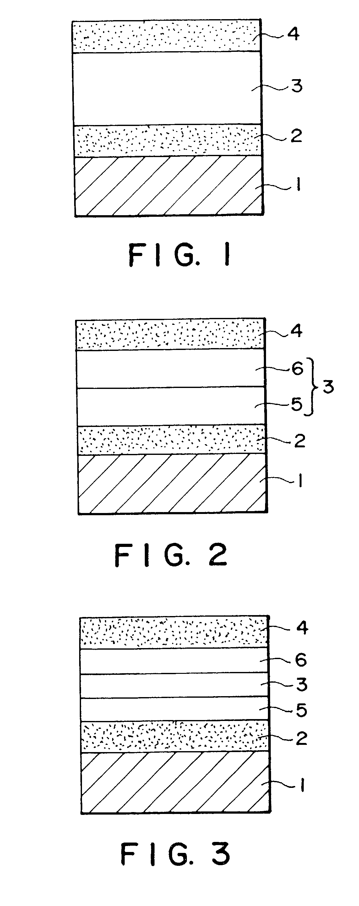
[0056] Thereafter, the polymerized film was coated by vacuum deposition successively with a 50 nm-thick film of Alq.sub.3 (electron-transporting luminescent layer 6) and a 150 nm-thick Al--Li alloy (cathode film 4) similarly as in Example 1 to form an organic luminescence device having a structure as shown in FIG. 2.

example 3

[0059] 1 wt. part of N,N'-diphenyl-N,N'-bis(4-vinylphenyl)-4,4'-diamino-1,-1'-biphenyl (DPDVDAB) and 1 wt. part of methoxyethylhexyl-p-phenylene-viny-lene (MEH-PPV) were dissolved in 148 wt. parts of para-xylene to form a coating liquid (solid content: 1.33 wt. %). The coating liquid was applied by spin coating (2000 rpm) on an ITO-coated transparent conductive substrate identical to the one used in Example 1, followed by drying at 80.degree. C. for 10 min. and heat-treatment at 120.degree. C. for 10 hours, respectively in a nitrogen atmosphere, to form a 70 nm-thick polymerized film.

[0060] Then, the polymerized film was coated with a 150 nm-thick cathode film (layer 4) of Al--Li alloy (Li content=1 atm. %) by vacuum deposition at a film growth rate of 1.0-1.2 nm / sec in a vacuum of 1.0.times.10.sup.-4 Pa to form an organic luminescence device having a structure as shown in FIG. 1.

[0061] The device was driven by applying a DC voltage of 10 volts between the ITO electrode 2 and the Al...

example 4

[0062] N,N,N',N'-tetrakis[3-methacryloyloxyphenyl]-4,4'-diamino-1,1'-biphe-nyl (TMDAB) and benzoyl peroxide (in 2 wt. % of TMDAB) were dissolved in toluene to form a 1.0 wt. %-coating liquid. The coating liquid was applied by spin coating (2000 rpm) on an ITO-coated transparent conductive substrate identical to the one used in Example 1, followed by drying at 80.degree. C. for 10 min. and heat-treatment at 120.degree. C. for 8 hours, respectively in a nitrogen atmosphere, to form a 65 nm-thick polymerized film (hole-transporting layer 5).

[0063] Then, 2,5-bis(4-styrylphenyl)-1,3,4-oxadiazole was dissolved in toluene to form a 1.0 wt. % coating liquid. The coating liquid was applied by spin-coating (2000 rpm) on the above formed hole-transporting layer (5), followed by drying at 80.degree. C. for 3 hours and heat-treatment at 120.degree. C. for 8 hours to form a 50 nm-thick polymerized film (electron-transporting luminescent layer 6).

[0064] Then, the polymerized film was coated with a...


PUM

PropertyMeasurementUnit
thicknessaaaaaaaaaa
thicknessaaaaaaaaaa
thicknessaaaaaaaaaa

Abstract

An organic luminescence device capable of luminescence at a high efficiency, a high luminance and high durability is formed by a pair of electrodes comprising an anode and a cathode, and at least one organic layer disposed between the electrodes. The at least one organic layer includes at least one layer comprising a polymerized film of organic layer having at least two polymerizable double bonds.

Description

FIELD OF THE INVENTION AND RELATED ART[0001] The present invention relates to an organic (electro-)luminescence device having a film of organic compound capable of light emission under application of an electric field, and a process for production thereof.[0002] An organic luminescence device generally comprises a pair of electrodes (comprising an anode and a cathode) and a film comprising a fluorescent organic compound disposed between the electrodes. Into the organic compound layer (film), holes and electrons are injected from the anode and the cathode, respectively, thus forming excitons of the fluorescent organic compound. When the excitons are returned to ground state, the organic luminescence device emits light or causes luminescence.[0003] According to a study by Eastman Kodak Co. ("Appl. Phys. Lett.", vol. 51, pp. 913-(1987)), it has been reported that a function-separation type organic luminescence layer comprising mutually laminated two layers including a layer of an alumi...

Claims


Application Information

Patent Timeline
Patent Type & Authority Applications(United States)
IPC IPC(8): H10K99/00C09K11/06H05B33/10
CPCH01L51/0035H01L51/0038H01L51/004H01L51/0043H01L51/0053H01L51/0054H01L51/0059H01L51/007H01L51/0071H01L51/0081H01L2251/308Y10T428/31855Y10T428/31909Y10T428/31931H10K85/111H10K85/114H10K85/141H10K85/151H10K85/621H10K85/622H10K85/6565H10K85/631H10K85/324H10K85/657H10K2102/103C09K11/06
Inventor SENOO, AKIHIROKAWAI, TATSUNDOOSATO, YOICHIHASHIMOTO, YUICHISUZUKI, KOICHITANABE, HIROSHIUENO, KAZUNORIMASHIMO, SEIJI
Owner CANON KK
Learn More