Image display apparatus having voltage application structure
a voltage application and display apparatus technology, applied in the manufacture of electric discharge tubes/lamps, tubes with screens, discharge tubes luminescnet screens, etc., can solve the problems of increased weight, difficult control of the area to which anode potential is applied, and fear of discharging
- Summary
- Abstract
- Description
- Claims
- Application Information
AI Technical Summary
Problems solved by technology
Method used
Image
Examples
first embodiment
[0070] First Embodiment
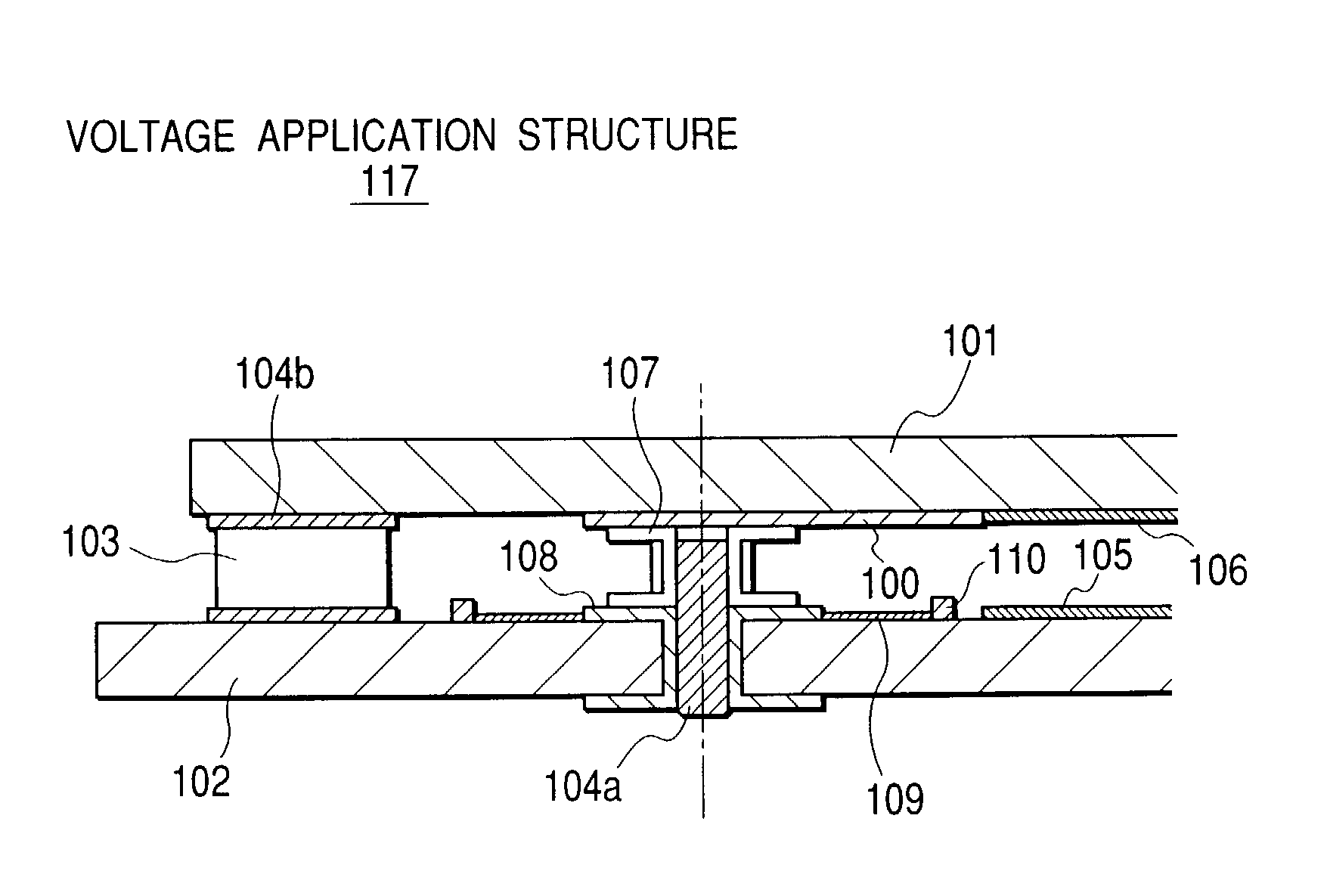
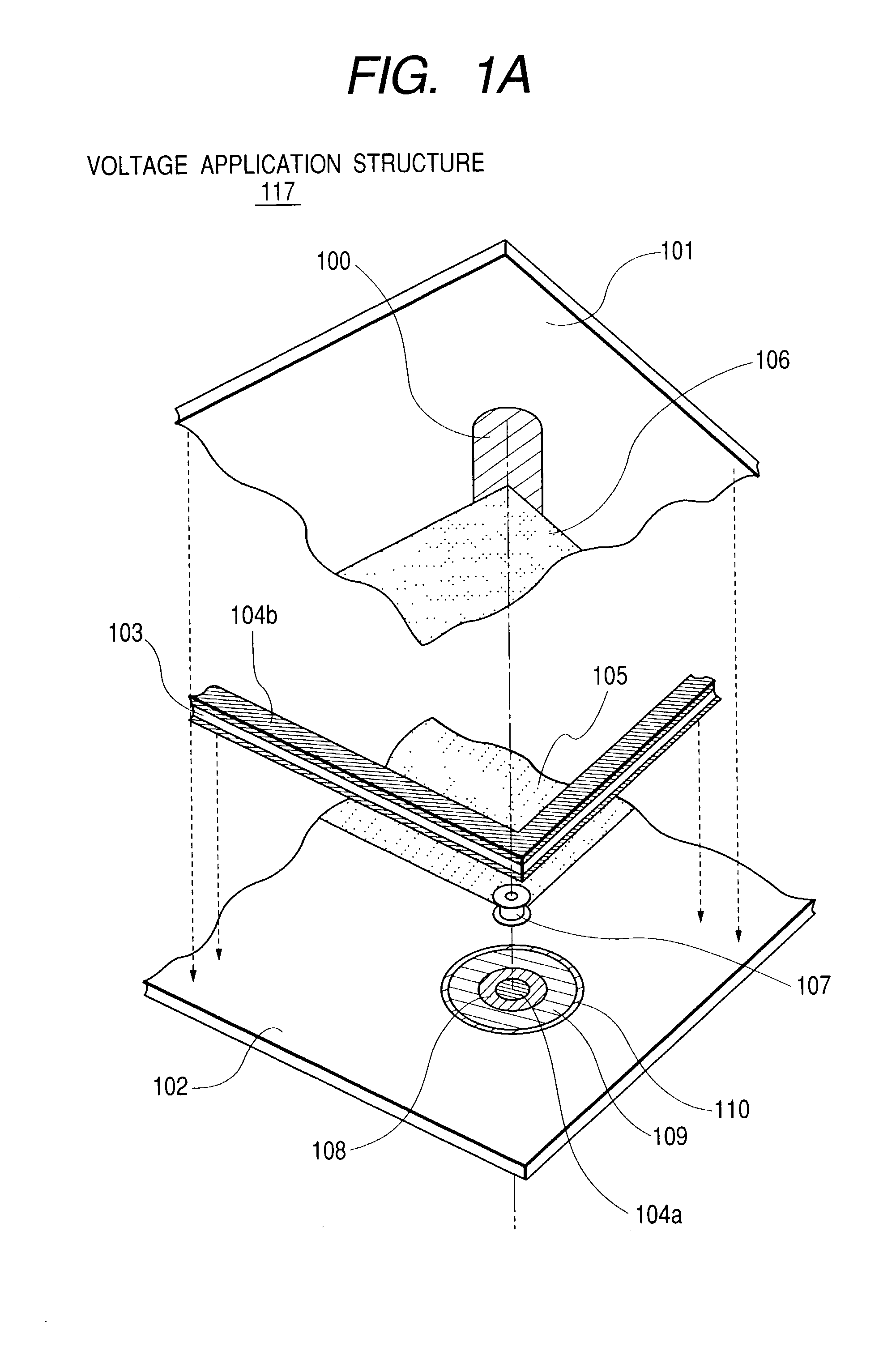
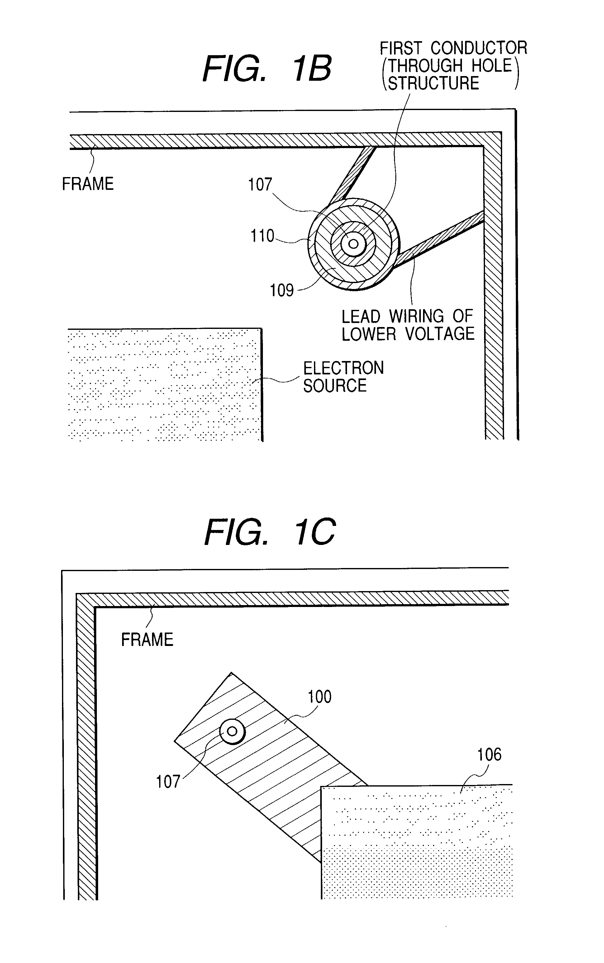
[0071] FIGS. 1A to 1C are each a disassembled perspective view of a first embodiment of the voltage application structure 117 of the present invention and a display apparatus using this voltage application structure. Also, FIG. 2 is an assembled sectional view of the first embodiment of the voltage application structure of the present invention and the display apparatus using this voltage application structure. Further, FIG. 4 shows the outline of the voltage application structure and the display apparatus using this voltage application structure shown in FIGS. 1A to 1C and 2. Note that FIG. 4 is a drawing viewed from a side (atmosphere side of the rear plate) opposite to a display portion (not shown) of the display apparatus (the enclosure is omitted in part for ease of explanation and there is shown the rear plate atmosphere side of the display panel).
[0072] When the display panel 113 of this embodiment is to be produced, first, a face plate 101, on whose su...
second embodiment
[0101] Second Embodiment
[0102] FIG. 6 is a disassembled perspective view of the second embodiment of the voltage application structure of the present invention and a display apparatus using this voltage application structure. Note that, a disassembled perspective view of the voltage application structure of the present invention and a display apparatus using this voltage application structure is the same as the one in FIG. 1A in the first embodiment. Also, a schematic view of the voltage application structure of the present invention and a display apparatus using this voltage application structure is the same as the one in FIG. 4 in the first embodiment.
[0103] Accordingly, there will be described in detail the elastic structure 207 that is a feature differenct from the first embodiment. Note that as to the reference numerals in FIG. 6, the same reference numerals are given to the same construction elements in FIG. 1. Also, other construction elements that are similar to those in FIG...
third embodiment
[0120] Third Embodiment
[0121] FIG. 7 is a disassembled perspective view of the third embodiment of the voltage application structure of the present invention and a display apparatus using this voltage application structure. Also, FIG. 8 is an assembled sectional view of the voltage application structure of the present invention and the display apparatus using this voltage application structure. Note that, a schematic view of the voltage application structure of the present invention and a display apparatus using this voltage application structure is the same as the one in FIG. 4 in the first and the second embodiments.
[0122] Accordingly, the elastic structure will be described below, which is a feature different between the preceding embodiments and this embodiment. The elastic structure 307 is placed between the through hole structure 108 on the rear plate 102 and the face plate 101. Note that the elastic structure 307 is constructed so as to be substantially axially symmetrical ab...
PUM
 Abstract
Description
Claims
Application Information
 - R&D
- Intellectual Property
- Life Sciences
- Materials
- Tech Scout
- Unparalleled Data Quality
- Higher Quality Content
- 60% Fewer Hallucinations
Browse by: Latest US Patents, China's latest patents, Technical Efficacy Thesaurus, Application Domain, Technology Topic, Popular Technical Reports.
© 2025 PatSnap. All rights reserved.Legal|Privacy policy|Modern Slavery Act Transparency Statement|Sitemap|About US| Contact US: help@patsnap.com


