Eureka AIR delivers breakthrough ideas for toughest innovation challenges, trusted by R&D personnel around the world.

Semiconductor device

a technology of semiconductor devices and circuits, applied in semiconductor devices, semiconductor/solid-state device details, electrical apparatus, etc., can solve the problems of poor layout efficiency, inconvenient for semiconductor devices, and loss due to electrical resistance, so as to maintain radiation performance, improve layout efficiency, and reduce the effect of loss

Inactive Publication Date: 2002-12-19
MITSUBISHI ELECTRIC CORP
View PDF0 Cites 64 Cited by
  • Summary
  • Abstract
  • Description
  • Claims
  • Application Information

AI Technical Summary

Problems solved by technology

In addition, the lead 207 is thin and the cross section area of the lead 207 and the cross section area of the circuit pattern on the printed circuit board for allowing a heavy current to flow to which the lead 207 is connected cannot be sufficiently secured and, therefore, the loss due to the electrical resistance cannot be ignored and there is the problem that the lead is not suitable for a semiconductor device for a heavy current.
However, the control circuit substrate 317 and the relay substrate 318 are separately provided on the metal substrate 304 and, therefore, layout efficiency is poor and there is the problem that miniaturization is difficult.
Therefore, the change ratio of the current becomes large in the case that the semiconductor element 301 is operated in a switching manner and, therefore, an element which withstands a high voltage must be prepared and this becomes a factor leading to an increase in the cost.
As described above, in a conventional semiconductor device, it is difficult to satisfy both the requirements concerning the radiation of heat and concerning miniaturization.
In addition, since the radiation performance can be maintained, the increase in temperature of the semiconductor device can be limited and, therefore, a greater selection of materials for the mold resin can be used and, therefore, less expensive mold resin can be utilized so as to reduce the cost.

Method used


Image

  • Semiconductor device
  • Semiconductor device
  • Semiconductor device

Examples


Embodiment Construction

[0158] FIG. 10 shows a cross section view of the configuration of the semiconductor device M201 as a modified example of the semiconductor device M200. The configuration of the semiconductor device M201 is essentially the same as that of the semiconductor device M200 which is described in reference to FIGS. 7 and 8 and the same symbols are attached to the same components and repetitive explanations are omitted.

[0159] The semiconductor device M201 is different from the semiconductor device M200 in the point that the bordering parts between the body part 23 1B and electrode protruding parts 232B are parts having curved surfaces RP with a curvature.

[0160] By adopting such a fillet structure in the case that the external conductors and the external connection electrode plates 8B are fastened with bolts in the electrode protruding parts 232B, the stress caused in the border parts between the body part 231B and the electrode protruding parts 232B becomes small even when the bolt is fasten...


PUM


Abstract

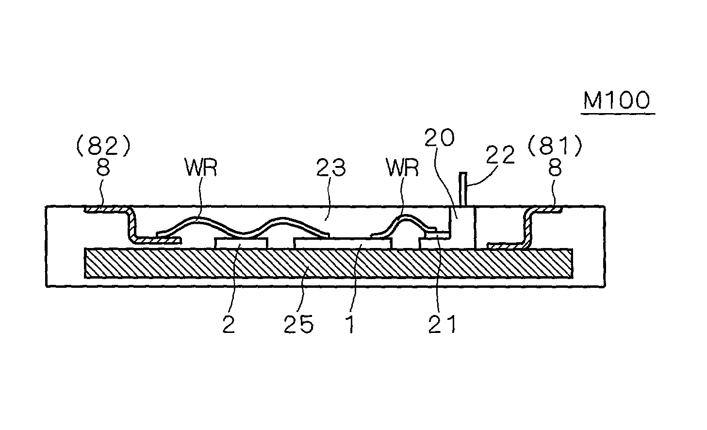
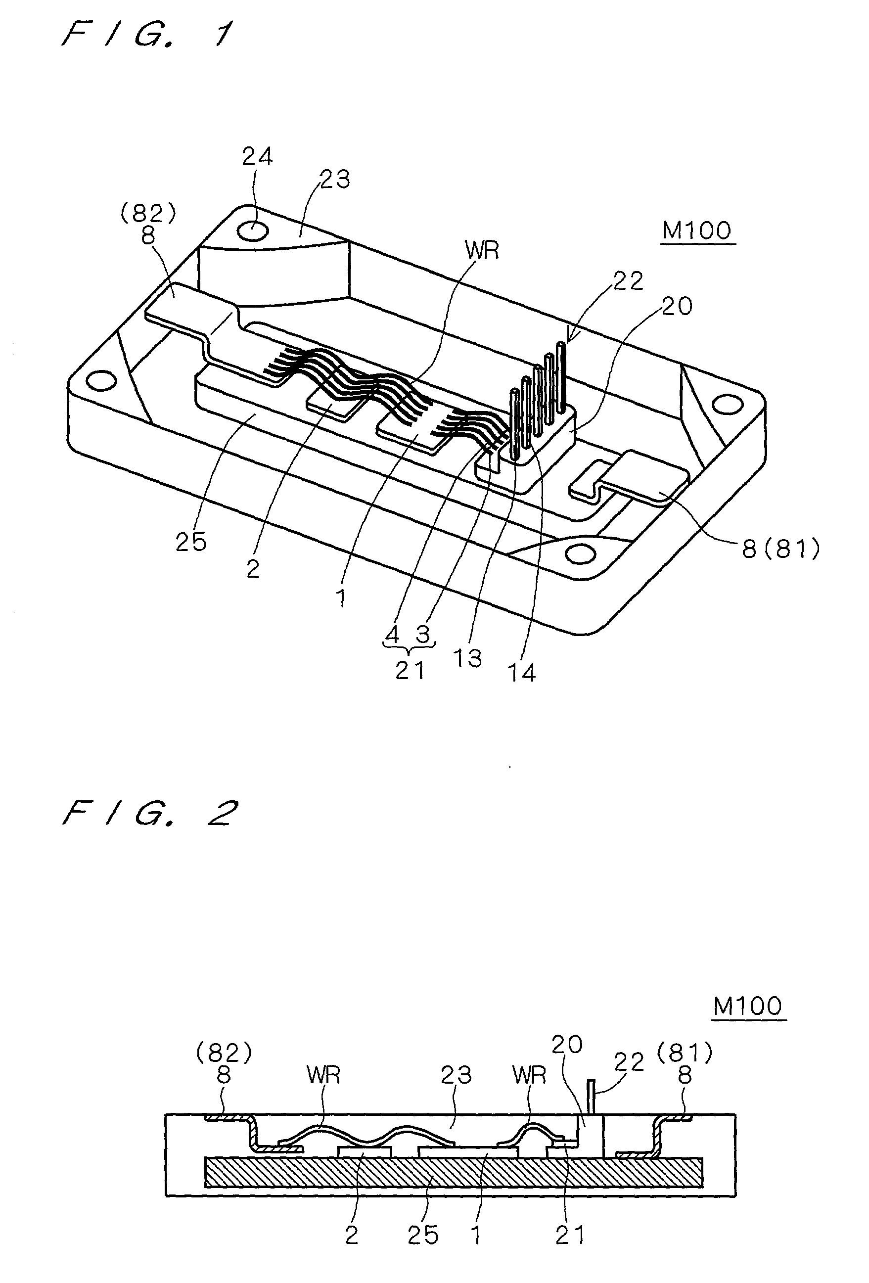
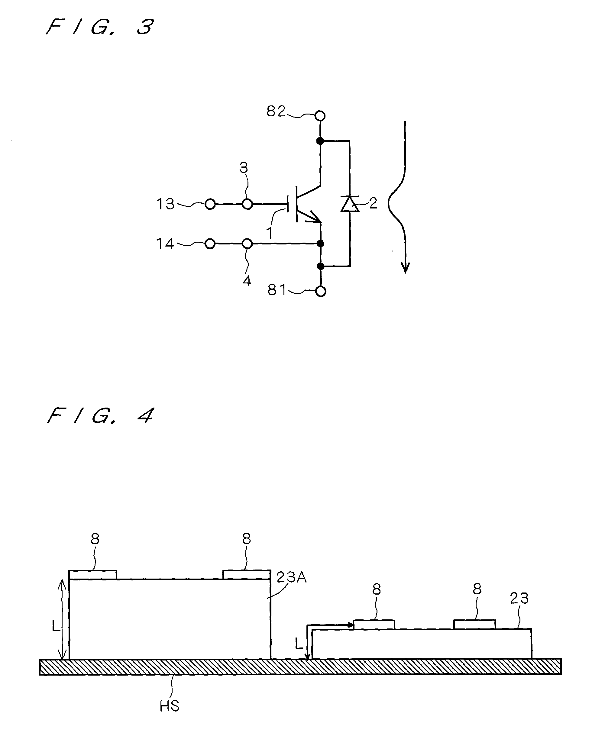
A semiconductor device which satisfies both the requirements for radiation performance and for miniaturization while having a semiconductor element for a heavy current. The semiconductor device has an IGBT element (1) and diode element (2) which are provided on the main surface of the heat spreader (25) in a strip form formed of a metal with excellent heat conductivity and electricity conductivity. In addition, a relay terminal block (20) is provided outside of the IGBT element (1) on the main surface of the heat spreader (25) and the relay terminal block (20), the IGBT element (1) and the diode element (2) are aligned. Then, the external connection electrode plates (81) and (82) are, respectively, provided on both sides of this alignment. The heat spreader (25), the IGBT element (1), the diode element (2), the relay terminal block (20) and the external connection electrode plate (8) are sealed in a resin of a box shape by using transfer molding and the resin package (23) defines the external form of the semiconductor device (M100).

Description

[0001] 1. Field of the Invention[0002] The present invention relates to a semiconductor device, in particular, to a semiconductor device for power which withstands a high voltage.[0003] 2. Description of the Background Art[0004] FIG. 29 shows a cross section view of the structure of the semiconductor device M70 as an example of a conventional semiconductor device. As shown in FIG. 29, in the semiconductor device M70, for example, an insulating substrate 102 is mounted on a base plate 104 formed of oxygen-free copper and a semiconductor element 101, which is a switching element, is mounted on this insulating substrate 102. On the insulating substrate 102, a predetermined conductor pattern is provided on one of the main surfaces of the insulating substrate and a semiconductor element, or the like, is provided on this conductor pattern. In addition, a conductor layer is provided on the other main surface so as to provide a structure that can be adhered to a conductor plate, or the like...

Claims


Application Information

Patent Timeline
Patent Type & Authority Applications(United States)
IPC IPC(8): H01L21/56H01L23/433H01L23/34H01L25/07H01L25/18
CPCH01L21/565H01L23/4334H01L24/45H01L24/49H01L25/072H01L25/18H01L2224/45124H01L2224/48091H01L2224/48137H01L2224/48247H01L2224/48472H01L2224/49175H01L2924/01004H01L2924/01005H01L2924/01006H01L2924/01013H01L2924/01014H01L2924/01015H01L2924/0102H01L2924/01029H01L2924/01074H01L2924/01079H01L2924/01082H01L2924/01093H01L2924/13055H01L2924/30107H01L2924/01019H01L2924/01023H01L2924/01033H01L2924/01068H01L2924/01076H01L2924/01084H01L2924/014H01L24/48H01L2224/45144H01L2224/49111H01L2224/48139H01L2924/19107H01L2224/32225H01L2224/73265H01L2924/1305H01L2924/00014H01L2924/00H01L2224/48227H01L2924/00012H01L2224/45015H01L2924/181H01L24/73H01L2924/00015
Inventor NAKAJIMA, DAICHUMA, HIDEAKI
Owner MITSUBISHI ELECTRIC CORP
Why Eureka
Eureka Blog
Learn More