Write buffer for use in a data processing apparatus

a data processing apparatus and write buffer technology, applied in the field of write buffers for use in data processing apparatuses, can solve problems such as adversely affecting the processing speed of the processor cor

Inactive Publication Date: 2002-03-28
ARM LTD
View PDF0 Cites 5 Cited by
  • Summary
  • Abstract
  • Description
  • Claims
  • Application Information

AI Technical Summary

Benefits of technology

[0021] In accordance with the present invention, each row of the write buffer is able to store either an address or a data value, an additional flag field is associated with each row, and the flag field is settable to indicate whether that row contains an address or a data value. Hence, in burst-mode, a particular row will be used to store the base address, with the flag field for that row being set accordingly to indicate that an address is contained within that row, and then subsequently the data values forming the burst traffic will be stored in other rows of the write buffer, with the flag fields of those rows being set to indicate that data values are contained within those rows. This approach makes very efficient use of the available write buffer area when buffering burst mode write traffic.
[0023] It has been found that a write buffer in accordance with the present invention can be arranged to occupy a relatively small area, whilst providing a good compromise between a write buffer optimized for non-burst mode traffic, and a write buffer optimized for burst mode traffic.

Problems solved by technology

Whilst the use of a cache improves the processing speed of the processor core, there is still the requirement for the processor core to read data values from, and write data values to, the memory, and these processes are relatively slow, thereby adversely affecting the processing speed of the processor core.
In such an arrangement, an address incrementer is typically required to re-synthesize the burst addresses as the contents of the write buffer are output to memory, and more complex control logic is required to interlock the address and data write buffer reconstruction.

Method used


Image

  • Write buffer for use in a data processing apparatus
  • Write buffer for use in a data processing apparatus
  • Write buffer for use in a data processing apparatus

Examples


Embodiment Construction

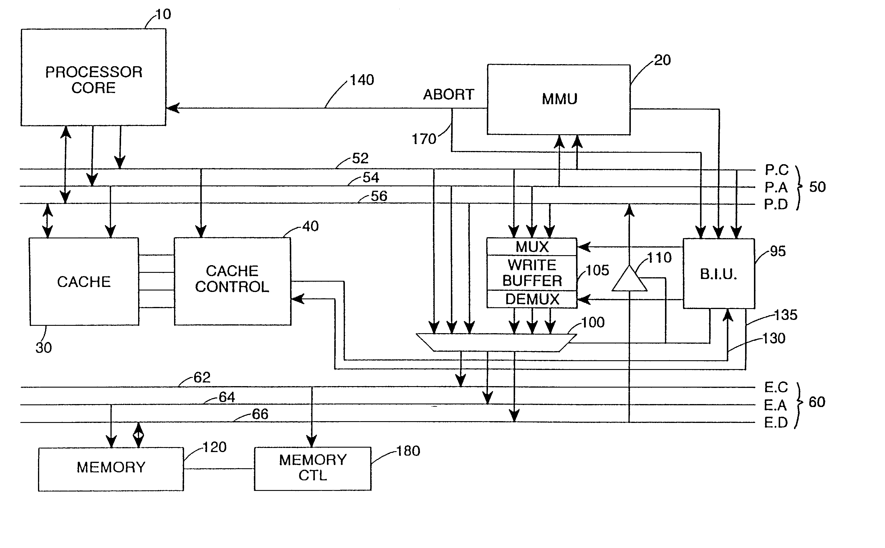
[0037] A data processing circuit in accordance with the preferred embodiment of the present invention will be described with reference to the block diagram of FIG. 1. As shown in FIG. 1, the data processing circuit has a processor core 10 arranged to process instructions received from memory 120. Data required by the processor core 10 for performing those instructions may also be retrieved from memory 120. A cache 30 is provided for storing data and instructions retrieved from the memory 120 so that it is subsequently readily accessible by the processor core 10. The cache control unit 40 is also provided to control the storage of instructions and data in the cache 30, and to control the retrieval of the data and instructions from the cache.

[0038] When the processor core 10 requires an instruction or an item of data (hereafter instructions or data will both be referred to as data values), it places the memory address of that data value on bus line 54 of processor bus 50. Further, the...


PUM


Abstract

The present invention provides a data processing apparatus comprising a processor core for generating addresses identifying locations in a memory and data values for storing in the memory, and a write buffer for storing the addresses and data values output by the processor core, and for subsequently outputting said addresses and data values to cause the data values to be stored in said memory. The write buffer comprises a plurality of rows, each row being arranged to store an address or data value, and each row having associated therewith a flag field settable to indicate whether that row contains an address or a data value. In accordance with the present invention, the write buffer provided by the data processing apparatus adaptively adjusts the number of rows it requires for addresses, and hence can be arranged to occupy a relatively small area, whilst still efficiently supporting both burst mode and non-burst mode write traffic.

Description

[0001] 1. Field of the Invention[0002] The present invention relates to a data processing apparatus for buffering addresses identifying locations in a memory, and data values to be written to those memory locations. The term `data value` is used herein to refer to both instructions and to items or blocks of data, such as data words.[0003] 2. Description of the Prior Art[0004] A typical data processing apparatus includes a processor core (or CPU) arranged to execute a sequence of instructions that are applied to data supplied to the processor core. Generally, a memory may be provided for storing the instructions and data (collectively referred to herein as "data values") required by the processor core. Further, it is often the case that one or more caches are provided for storing data values required by the processor core, so as to reduce the number of accesses required to the memory.[0005] Whilst the use of a cache improves the processing speed of the processor core, there is still ...

Claims


Application Information

Patent Timeline
Patent Type & Authority Applications(United States)
IPC IPC(8): G06F5/12G06F12/00G06F12/08G06F12/0879G06F12/10G06F12/1045G06F13/42
CPCG06F12/0879G06F12/1063G06F13/4243
Inventor FLYNN, DAVID WALTER
Owner ARM LTD
Why Eureka
Try Eureka