Power amplifier circuit
a power amplifier and circuit technology, applied in the direction of amplifiers, amplifiers with coupling networks, amplifiers with semiconductor devices/discharge tubes, etc., can solve the problem of not enough studies on a method for high-efficiency power amplification
- Summary
- Abstract
- Description
- Claims
- Application Information
AI Technical Summary
Benefits of technology
Problems solved by technology
Method used
Image
Examples
first embodiment
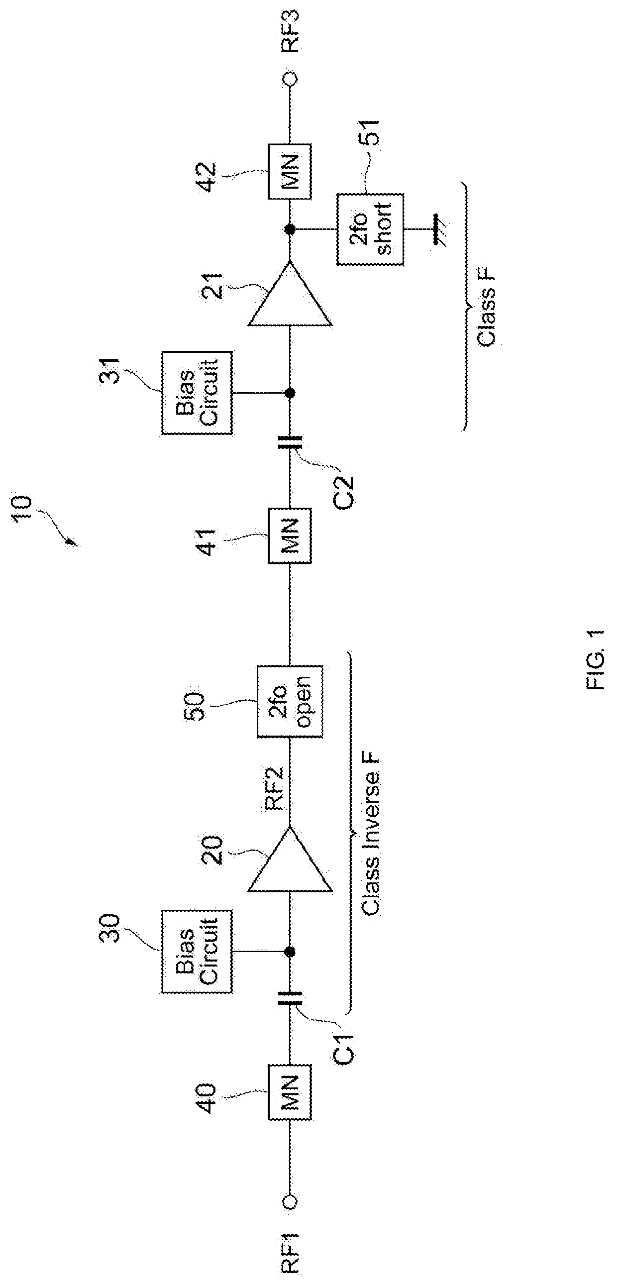
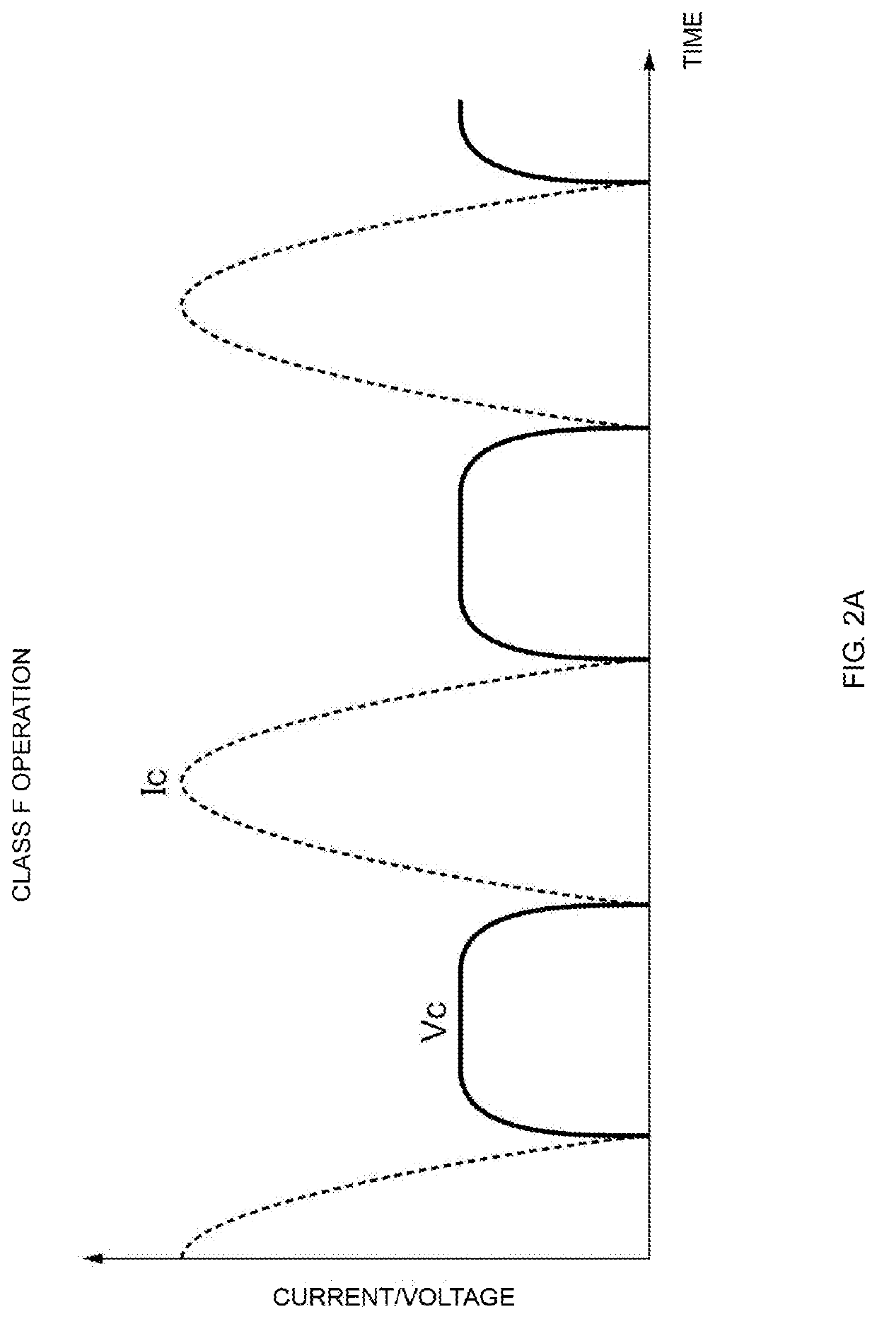
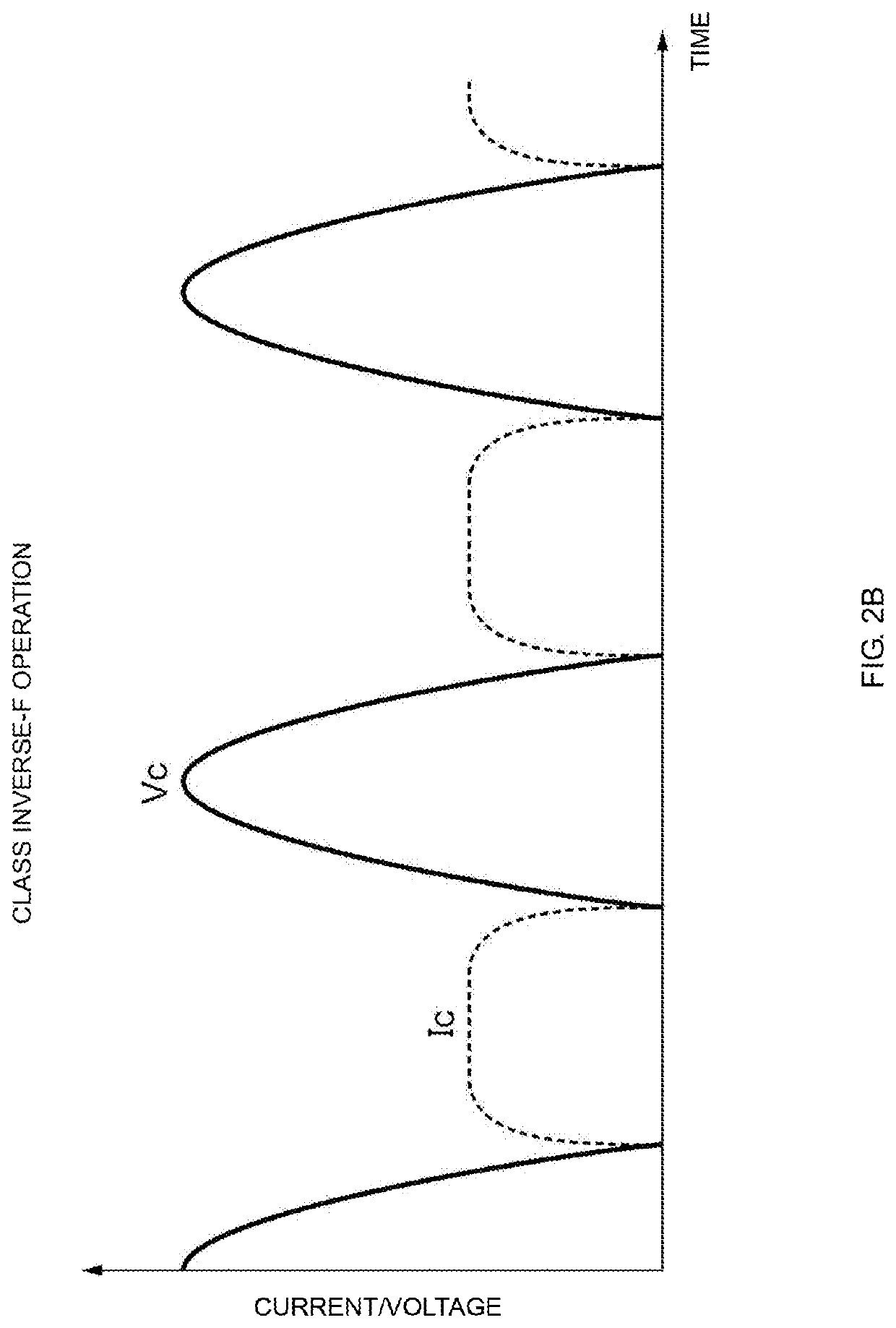
[0024]FIG. 1 illustrates an example configuration of a power amplifier circuit 10 according to the present disclosure. The power amplifier circuit 10 is mounted in, for example, a mobile communication device such as a mobile phone and is used to amplify the power of a radio-frequency (RF) signal to be transmitted to a base station. For example, the power amplifier circuit 10 amplifies transmission signals conforming to communication standards such as the second-generation mobile communication system (2G), the third-generation mobile communication system (3G), the fourth-generation mobile communication system (4G), the fifth-generation mobile communication system (5G), Long Term Evolution Frequency Division Duplex (LTE-FDD), LTE Time Division Duplex (LTE-TDD), LTE-Advanced, and LTE-Advanced Pro. The RF signal has a frequency of about several hundreds of megahertz (MHz) to about several tens of gigahertz (GHz), for example. The power amplifier circuit 10 may amplify signals having oth...
second embodiment
[0063]FIG. 10 illustrates the circuit configuration of a power amplifier circuit 10D according to the present disclosure.
[0064]As illustrated in FIG. 10, in the power amplifier circuit 10D, the configuration of the subsequent amplifier 21 is different from that in the embodiment described above. Specifically, unlike the power amplifier circuit 10A, the power amplifier circuit 10D includes a transistor Q3, a bias circuit 32, an adjustment circuit 60, a capacitor C9, and inductors L6 and L7. In FIG. 10, capacitors corresponding to the capacitors C3 and C4 illustrated in FIG. 3 are not illustrated.
[0065]As in the embodiment described above, the transistor Q2 (lower transistor) has a collector (first terminal) to which the power supply voltage Vcc (second power supply voltage) is supplied via the inductor L2, an emitter (second terminal) connected to ground, and a base (third terminal) to which the RF signal RF2 (second signal) is supplied via the capacitor C2.
[0066]The transistor Q3 (u...
PUM
 Abstract
Description
Claims
Application Information
 - R&D
- Intellectual Property
- Life Sciences
- Materials
- Tech Scout
- Unparalleled Data Quality
- Higher Quality Content
- 60% Fewer Hallucinations
Browse by: Latest US Patents, China's latest patents, Technical Efficacy Thesaurus, Application Domain, Technology Topic, Popular Technical Reports.
© 2025 PatSnap. All rights reserved.Legal|Privacy policy|Modern Slavery Act Transparency Statement|Sitemap|About US| Contact US: help@patsnap.com


