Automated analog layout

a technology of analog layout and automatic layout, applied in the field of electronic design automation for integrated circuits, can solve problems such as and achieve the effect of speeding up the entire design cycle and delivering layout results so quickly

Active Publication Date: 2022-03-22
PULSIC
View PDF30 Cites 1 Cited by
  • Summary
  • Abstract
  • Description
  • Claims
  • Application Information

AI Technical Summary

Benefits of technology

[0010]Some benefits of Pulsic Animate include: gets designers up to speed rapidly with minimal training and setup; reduces layout time from days or weeks to minutes; enables exploration of multiple architectures and extraction of realistic parasitics; creates manual-quality results in a fraction of the time; enables accurate simulation early in the design process; and uses native OpenAccess and PCells or PyCells.
[0011]Some features of Pulsic Animate include: easy-to-use GUI; automatic constraint recognition from schematics; unique PolyMorphic Layout technology generates multiple electrically correct layouts ranked by user-specified criteria; supports both CMOS digital (row-based) and CMOS analog (area-based) designs; and supports flat or hierarchical designs.

Problems solved by technology

Because the tool produces layout results so quickly, parasitics are available for simulation early in the design process, further speeding the entire design cycle.

Method used


Image

  • Automated analog layout
  • Automated analog layout
  • Automated analog layout

Examples


Embodiment Construction

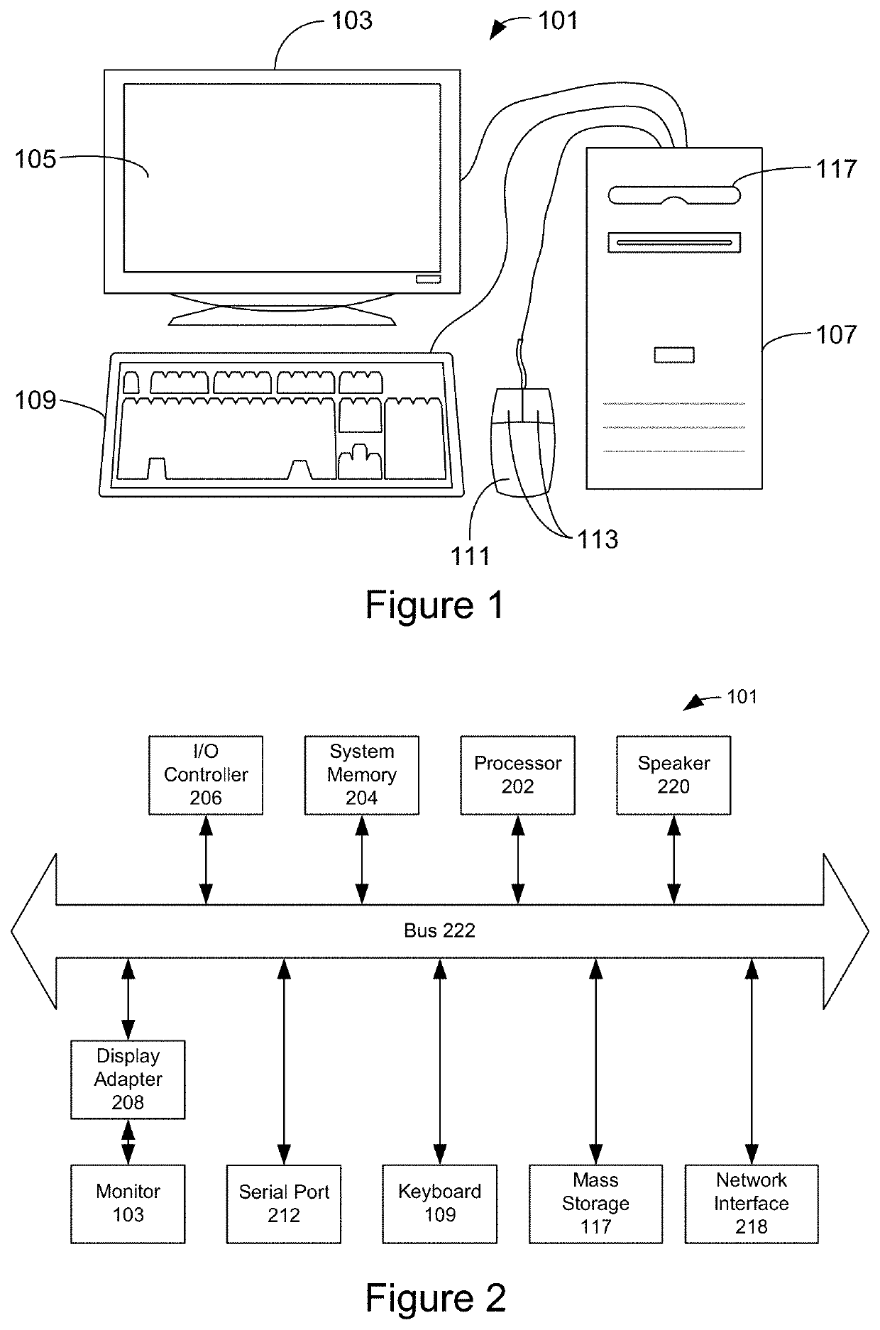
[0056]FIG. 1 shows an electronic design automation (EDA) system of the present invention for designing an electronic circuit or integrated circuit, including automated analog layout. In an embodiment, the invention is software that executes on a computer workstation system, such as shown in FIG. 1. FIG. 1 shows a computer system 101 that includes a monitor 103, screen 105, enclosure 107, keyboard 109, and mouse 111. Mouse 111 may have one or more buttons such as mouse buttons 113. Enclosure 107 (may also be referred to as a system unit, cabinet, or case) houses familiar computer components, some of which are not shown, such as a processor, memory, mass storage devices 117, and the like.

[0057]Mass storage devices 117 may include mass disk drives, floppy disks, magnetic disks, optical disks, magneto-optical disks, fixed disks, hard disks, CD-ROMs, recordable CDs, DVDs, recordable DVDs (e.g., DVD-R, DVD+R, DVD-RW, DVD+RW, HD-DVD, or Blu-ray Disc), flash and other nonvolatile solid-stat...


PUM


Abstract

An automated analog layout tool creates not just one, but many electrically correct layouts from an input schematic. Designers can explore multiple layout options in a fraction of the time needed to produce just a single layout by hand. Because the tool produces layout results so quickly, parasitics are available for simulation early in the design process, further speeding the entire design cycle. The tool considers place and route concurrently.

Description

CROSS-REFERENCE TO RELATED APPLICATIONS[0001]This patent application is a continuation of U.S. patent application Ser. No. 15 / 162,458, filed May 23, 2016, which claims priority to U.S. patent application 62 / 165,102, filed May 21, 2015. These applications are incorporated by reference along with all other references cited in this application.BACKGROUND OF THE INVENTION[0002]The present invention relates to the field of electronic design automation for integrated circuits, and in particular, to analog design automation.[0003]Integrated circuits are important building blocks of the information age and are critical to the information age, affecting every industry including financial, banking, legal, military, high technology, transportation, telephony, oil, medical, drug, food, agriculture, education, and many others. Integrated circuits such as DSPs, amplifiers, voltage converters, DRAMs, SRAMs, EPROMs, EEPROMs, Flash memories, microprocessors, ASICs, and programmable logic are used in...

Claims


Application Information

Patent Timeline
Patent Type & Authority Patents(United States)
IPC IPC(8): G06F30/327G06F30/394G06F30/392G06F111/12
CPCG06F30/327G06F30/392G06F30/394G06F2111/12
Inventor CLEWES, PAULGAO, LIANGLONGRIGG, JONATHAN
Owner PULSIC
Why Eureka
Try Eureka