Thin film capacitor and circuit board incorporating the same

a thin film capacitor and circuit board technology, applied in the direction of printed capacitor incorporation, cross-talk/noise/interference reduction, printed circuit stress/warp reduction, etc., can solve the problem of insufficient space on the circuit board for mounting many laminated ceramic chip capacitors, easy warpage, etc., to reduce the warpage of thin film capacitors that may occur when embedded in the circuit board, suppress warpage, and reduce warpage

Active Publication Date: 2022-02-01
TDK CORPARATION
View PDF9 Cites 0 Cited by
  • Summary
  • Abstract
  • Description
  • Claims
  • Application Information

AI Technical Summary

Benefits of technology

[0005]It is therefore an object of the present invention to provide a thin film capacitor whose warpage can be suppressed without making the thicknesses or materials of metal films formed on the front and back sides of a capacitive insulating film the same as each other and a circuit board incorporating the thin film capacitor.
[0008]According to the present invention, since the opening that penetrates the capacitive insulating film, first metal film and second metal film is formed, stress due to a difference in thickness or metal material between the first and second metal films is released through the opening. In addition, the second metal film is made thicker than the first metal film, and the first size is made larger than the second size, so that rigidity is ensured by the thicker second metal film, thereby significantly suppressing warpage. Thus, warpage of the thin film capacitor that may occur when it is embedded in the circuit board can be minimized.
[0009]In the thin film capacitor according to the present invention, the opening may comprise a plurality of openings, and assuming that an area where the capacitive insulating film is sandwiched between the first and second metal films in a plan view is a capacitive area and that an area where the capacitive insulating film is not present and an area where the capacitive insulating film is not sandwiched between the first and second metal films in a plan view is a non-capacitive area, the ratio of the capacitive area to the sum of the capacitive area and non-capacitive area may be set to 80% or less. This allows further suppression of warpage that may occur in the thin film capacitor.
[0010]In the present invention, assuming that the size of a part of the opening that penetrates the capacitive insulating film is a third size, the third size may be smaller than the first size. In addition, assuming that the size of a part of the opening that penetrates the second metal film at the boundary of the capacitive insulating film is a fourth size, the third size may be smaller than the fourth size. This increases the creepage distance between the first and second metal films inside the opening, thereby making it possible to improve withstand voltage.
[0011]In the present invention, the opening may be filled with an insulating material. This can improve product reliability.
[0012]As described above, according to the present invention, there can be provided a thin film capacitor whose warpage can be suppressed without making the thicknesses or materials of metal films formed on the front and back sides of a capacitive insulating film the same as each other and a circuit board incorporating the thin film capacitor.

Problems solved by technology

However, in recent years, it is often the case that a space on a circuit board for mounting many laminated ceramic chip capacitors is insufficient.
However, when the thin film capacitor is reduced in thickness, it may be easily warped.
To prevent the warpage of the thin film capacitor, the thicknesses and materials of metal films formed on the front and back sides of a capacitive insulating film are made the same as each other; however, it is not realistic to make the thicknesses and materials thereof the same as each other.

Method used


Image

  • Thin film capacitor and circuit board incorporating the same
  • Thin film capacitor and circuit board incorporating the same
  • Thin film capacitor and circuit board incorporating the same

Examples


first embodiment

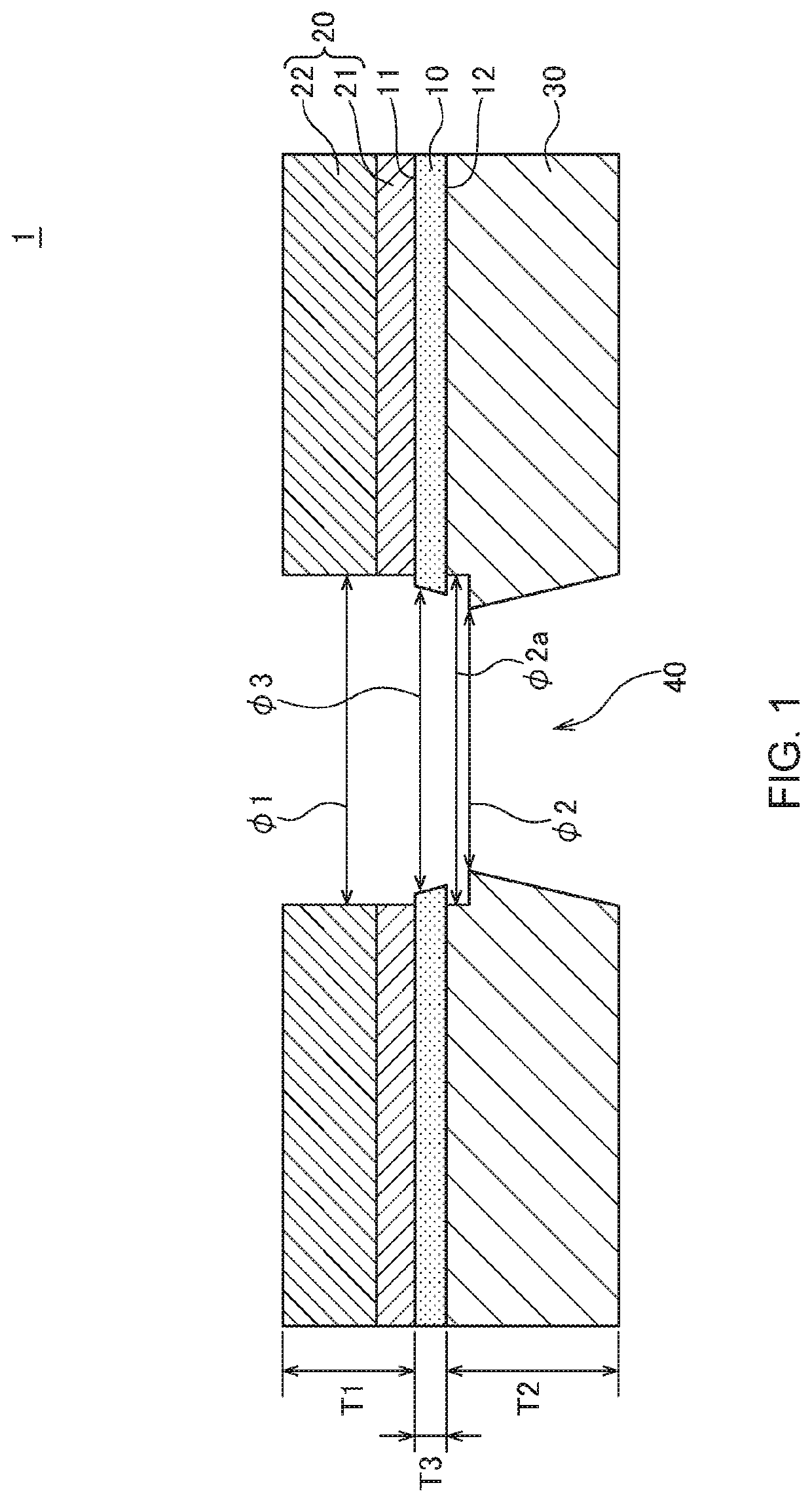
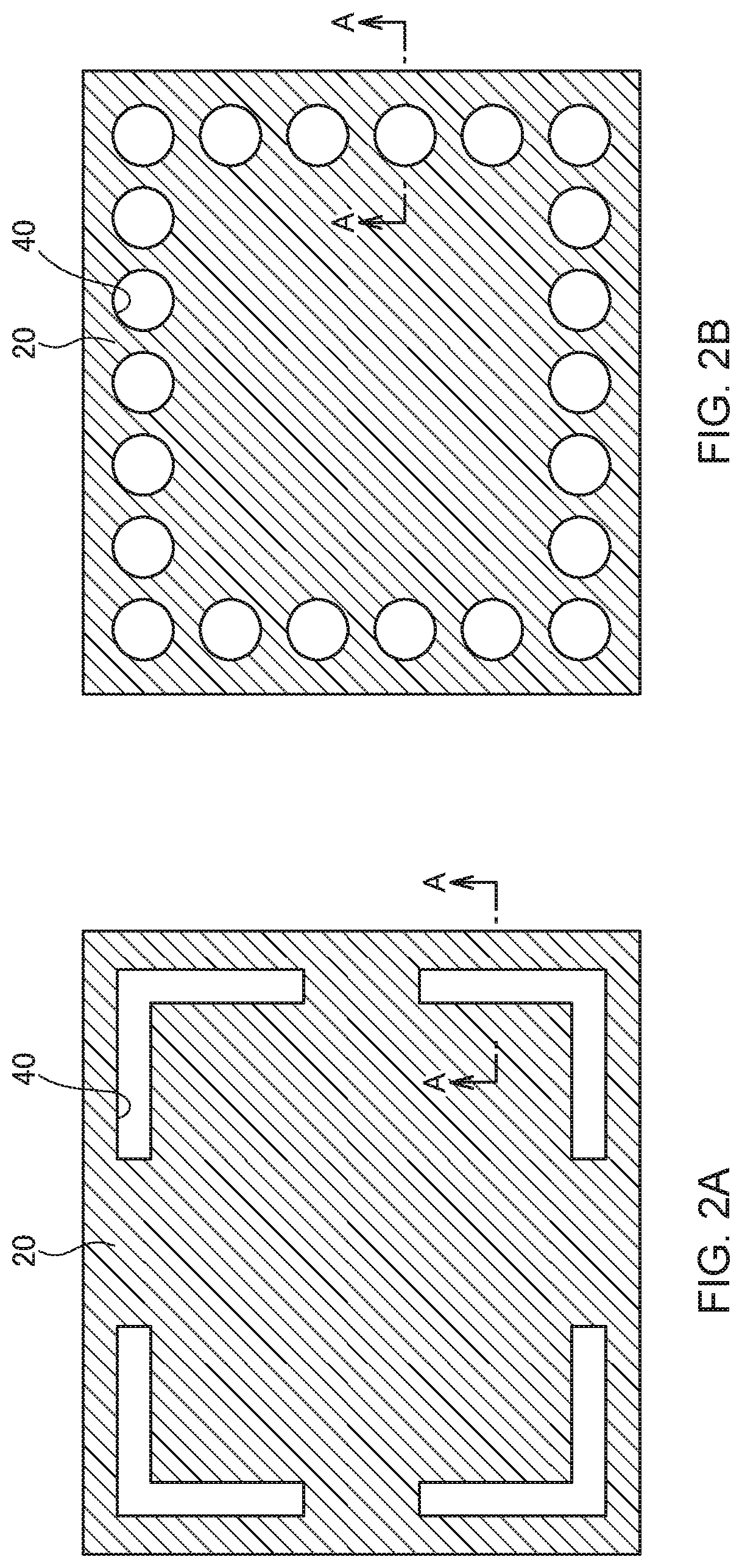
[0025]FIG. 1 is a schematic cross-sectional view for explaining the configuration of a thin film capacitor 1 according to the first embodiment of the present invention. FIGS. 2A and 2B are partial plan views of the thin film capacitor 1 and illustrate a first example and a second example, respectively. The cross section illustrated in FIG. 1 corresponds to that taken along line A-A in FIG. 2.

[0026]As illustrated in FIGS. 1 and 2A and 2B, the thin film capacitor 1 according to the present embodiment includes a capacitive insulating film 10, a first metal film 20 formed on one surface 11 of the capacitive insulating film 10, and a second metal film 30 formed on the other surface 12 of the capacitive insulating film 10. The capacitive insulating film 10 is made of a ceramic material having a perovskite structure, such as barium titanate. The metal film 20 has a structure in which a seed layer 21 and a plated film 22 are laminated. The seed layer 21 is made of, e.g., a laminated film of...

second embodiment

[0047]FIG. 10 is a schematic cross-sectional view for explaining the configuration of a thin film capacitor 2 according to the second embodiment of the present invention. The planar shape of the thin film capacitor 2 according to the present embodiment is as illustrated in FIGS. 2A and 2B.

[0048]As illustrated in FIG. 10, the thin film capacitor 2 according to the second embodiment differs from the thin film capacitor 1 according to the first embodiment in that the inside of the opening 40 is filled with insulating resin 50. Other basic configurations are the same as those of the thin film capacitor 1 according to the first embodiment, so the same reference numerals are given to the same elements, and overlapping description will be omitted.

[0049]The following describes a manufacturing method for the thin film capacitor 2 according to the present embodiment.

[0050]FIGS. 11 to 13 are process views illustrating a manufacturing method for the thin film capacitor 2 according to the presen...

third embodiment

[0055]FIG. 14 is a schematic cross-sectional view for explaining the configuration of a thin film capacitor 3 according to the third embodiment of the present invention. The planar shape of the thin film capacitor 3 according to the present embodiment is as illustrated in FIGS. 2A and 2B.

[0056]As illustrated in FIG. 14, the basic configuration of the thin film capacitor 3 according to the third embodiment is the same as that of the thin film capacitor 1 according to the first embodiment. That is, the thickness T2 of the metal film 30 formed on the surface 12 of the capacitive insulating film 10 is larger than the thickness T1 of the metal film 20 formed on the surface 11 of the capacitive insulating film 10, and the size ϕ1 of the opening 40 in the metal film 20 is larger than the size ϕ2 of the opening 40 in the metal film 30. However, in the thin film capacitor 3 according to the present embodiment, the opening 40 formed in the metal film 30 is tapered in a form reversal of the op...


PUM

PropertyMeasurementUnit
sizesaaaaaaaaaa
sizesaaaaaaaaaa
thickness T3aaaaaaaaaa

Abstract

Disclosed herein is a thin film capacitor that includes a capacitive insulating film, a first metal film formed on one surface of the capacitive insulating film, and a second metal film formed on other surface of the capacitive insulating film and made of a metal material different from that of the first metal film. The thin film capacitor has an opening penetrating the capacitive insulating film, first metal film, and second metal film. The second metal film is thicker than the first metal film. A first size of a part of the opening that penetrates the first metal film is larger than a second size of a part of the opening that penetrates the second metal film.

Description

BACKGROUND OF THE INVENTIONField of the Invention[0001]The present invention relates to a thin film capacitor and a circuit board incorporating the thin film capacitor and, more particularly, to a thin film capacitor capable of being embedded in a circuit board and used and a circuit board incorporating the thin film capacitor.Description of Related Art[0002]In general, a decoupling capacitor is mounted on a circuit board on which an IC is mounted for stabilizing the potential of a power supply to be fed to the IC. A laminated ceramic chip capacitor is generally used as the decoupling capacitor, and a required decoupling capacitance is ensured by mounting many laminated ceramic chip capacitors on the surface of a circuit board.[0003]However, in recent years, it is often the case that a space on a circuit board for mounting many laminated ceramic chip capacitors is insufficient. Thus, there has been proposed a method of using a thin film capacitor in place of the laminated ceramic ch...

Claims


Application Information

Patent Timeline
Patent Type & Authority Patents(United States)
IPC IPC(8): H05K1/00H05K1/02H05K1/11H05K1/16
CPCH05K1/0231H05K1/113H05K1/162H05K2201/0179H05K3/007H05K2201/09154H05K1/0271H05K2201/0352H05K2201/09827H05K2201/09845
Inventor YOSHIKAWA, KAZUHIROABURAKAWA, YUUKINAMIKAWA, TATSUOYOSHIDA, KENICHISAITA, HITOSHI
Owner TDK CORPARATION
Why Eureka
Try Eureka