
Display device with current compensation and manufacturing method thereof

a display device and compensation technology, applied in the field of display devices, can solve the problems of affecting the performance of the product, limiting the application of the two-layer source/drain structure, etc., and achieve the effects of narrow application range, uneven brightness of the display device, and high cos

Active Publication Date: 2022-02-01
WUHAN CHINA STAR OPTOELECTRONICS SEMICON DISPLAY TECH CO LTD
View PDF22 Cites 0 Cited by
  • Summary
  • Abstract
  • Description
  • Claims
  • Application Information

AI Technical Summary

Benefits of technology

This patent is trying to solve the problem of manufacturing a display device with two layers of source / drain structures that are complicated and costly. The patent provides a solution that makes the display brighter and evenly distributed. The method used is called current compensation, which gradually increases the capacitance value of the storage capacitor from the vicinity of the integrated circuit area to the direction away from the integrated circuit area. This results in a gradual decrease in input current and voltage, which improves the uneven brightness of the display. Overall, this patent simplifies the manufacturing process, reduces the cost, and makes the display device more widely applicable.

Problems solved by technology

Therefore, brightness of the two ends of the display area is significantly different, and the display device has uneven brightness, which affects performance of the product.
However, the design of the two-layer source / drain structure restricts its application due to the complicated manufacturing process and high cost.

Method used


Image

  • Display device with current compensation and manufacturing method thereof
  • Display device with current compensation and manufacturing method thereof
  • Display device with current compensation and manufacturing method thereof

Examples


Embodiment Construction

[0028]Structure and technical means adopted by the present disclosure to achieve the above and other objects can be best understood by referring to the following detailed description of the preferred embodiments and the accompanying drawings. Furthermore, directional terms described by the present disclosure, such as upper, lower, front, back, left, right, inner, outer, side, longitudinal / vertical, transverse / horizontal, etc., are only directions by referring to the accompanying drawings, and thus the used directional terms are used to describe and understand the present disclosure, but the present disclosure is not limited thereto.

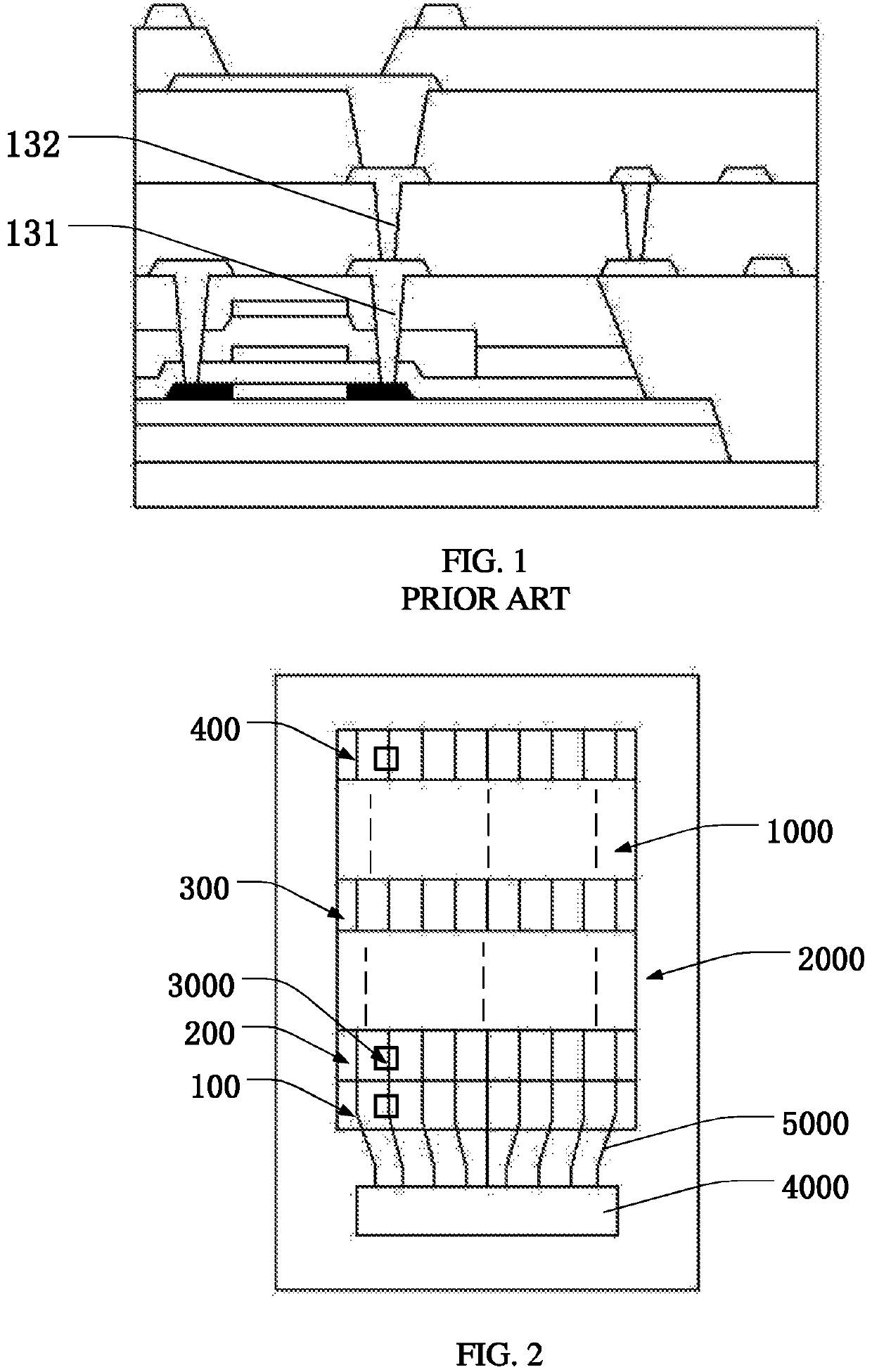
[0029]Referring to FIG. 2, a display device is provided according to an embodiment of the present disclosure. The display device comprises a display area 1000 and a non-display area 2000, and the display area 1000 is surrounded by the non-display area 2000. The non-display area 2000 includes an integrated circuit area 4000 (IC chip). Operational signals a...


PUM

PropertyMeasurementUnit
thicknessaaaaaaaaaa
capacitanceaaaaaaaaaa
insulatingaaaaaaaaaa

Abstract

A display device and a manufacturing method thereof. The display device includes a display area and a non-display area. The display area includes a substrate, a first insulating layer, a first gate layer, a second insulating layer, and a second gate layer. The non-display area includes an integrated circuit area, and a thickness of the second insulating layer is gradually decreased from a vicinity of the integrated circuit area toward a direction away from the integrated circuit area. The manufacturing method of the display device includes a preparation step of disposing a substrate, a preparation step of disposing a first insulating layer, a preparation step of disposing a first gate layer, a preparation step of disposing a second insulating layer, and a preparation step of disposing a second gate layer.

Description

FIELD OF INVENTION[0001]The present disclosure relates to a display field, in particular, relates to a display device and a manufacturing method thereof.BACKGROUND OF INVENTION[0002]Organic light emitting diode (OLED) display devices have unique advantages of low power consumption, high saturation, fast response times, and wide viewing angles, and has gradually become the mainstream technology in the display field. It has a wide applications in cars, mobile phones, tablets, computers, and TV products.[0003]One mainstream driving method of the OLED display device is current driving, wherein operating current is transmitted by the display device through a source / drain. There is a certain resistance in the source / drain, and there is a voltage drop (IR Drop) in signal transmission. In the display area, the voltage and current in the area close to the driving circuit are large, and the voltage and current in the area away from the driving circuit are small. Therefore, brightness of the t...

Claims


Application Information

Patent Timeline
Patent Type & Authority Patents(United States)
IPC IPC(8): H01L29/08H01L27/32H01L51/56
CPCH01L27/3244H01L51/56H01L2227/323H01L21/77H01L27/12G02F1/1362H10K59/124H10K59/1216H10K59/1315H10K59/12H10K71/00H10K59/1201
Inventor FANG, LIANGDING, DING
Owner WUHAN CHINA STAR OPTOELECTRONICS SEMICON DISPLAY TECH CO LTD
Learn More