Optical modulation element
a technology of optical modulation and element, applied in the field of light modulation element, can solve the problems of deteriorating product quality, generating bends on the surfaces of the upper and lower base films, etc., and achieve the effect of improving the surface reducing the waviness of the upper base film, and improving the quality of the produ
- Summary
- Abstract
- Description
- Claims
- Application Information
AI Technical Summary
Benefits of technology
Problems solved by technology
Method used
Image
Examples
example 1
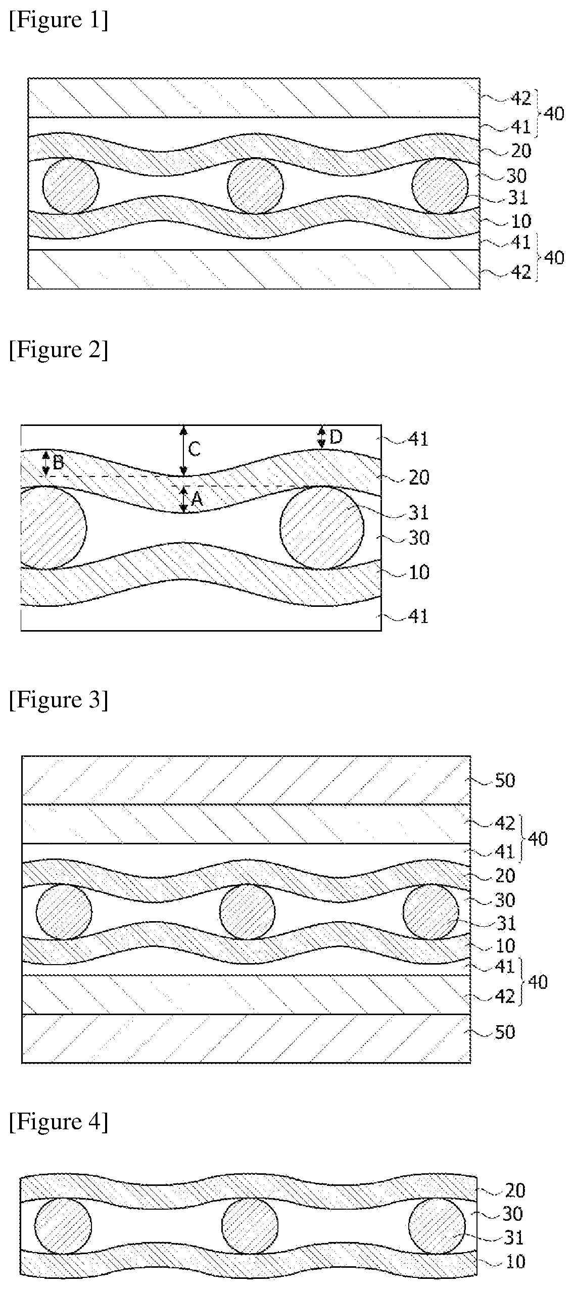
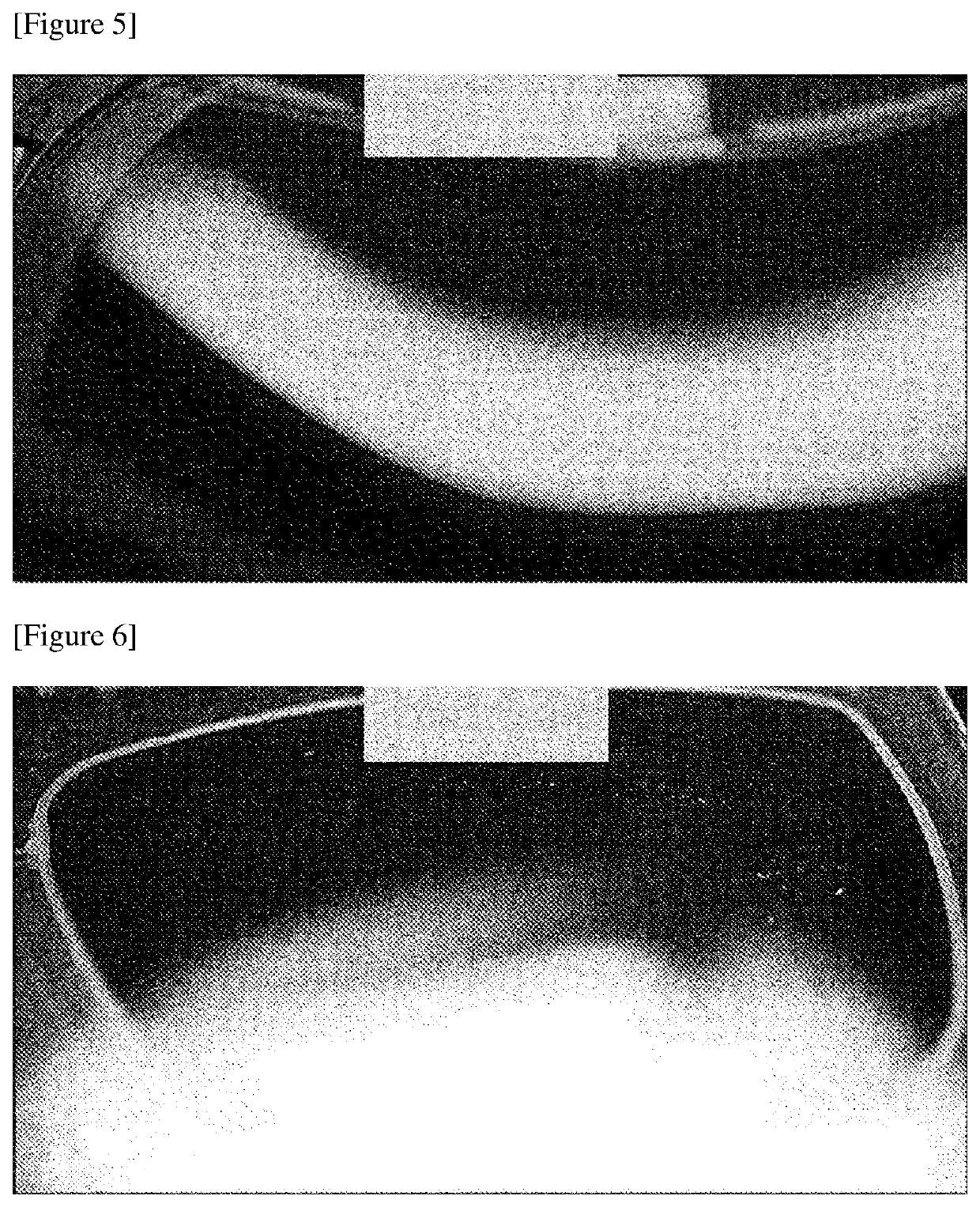
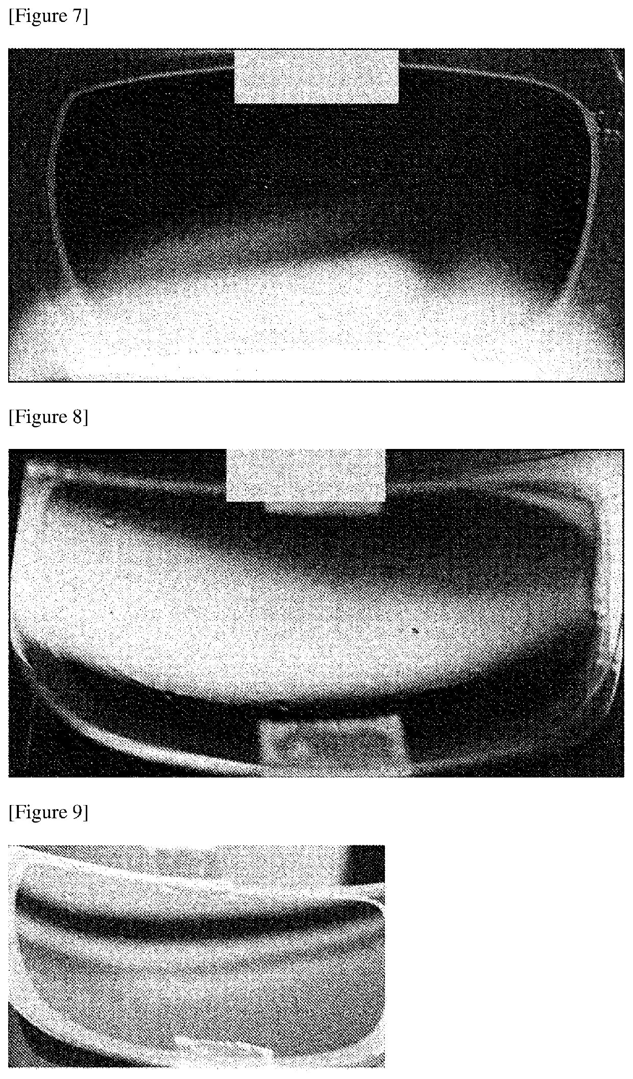
[0064]As a light modulation element of Example 1, a light modulation element having an eyewear lens shape was produced. Specifically, as a film on which an electrode layer was formed on each of first and second base films, a PC-ITO film (Teijin) having a total thickness of 100 μm, in which an ITO layer was deposited on a PC film, was prepared. A composition comprising a liquid crystal compound (MDA-16-1235, Merck) and a ball spacer (KBN-512, Sekisui Co.) having a particle diameter of 12 μm was applied on the electrode layer of the first base film to form a light modulating layer. At this time, the composition was applied on the PC-ITO film in the inner region of an outer sealant applied in the edge shape of the eyewear lens. After the second base film was laminated so that the electrode layer of the second base film was in contact with the light modulating layer, the surface waviness was formed on both surfaces of the first base film and the second base film due to the difference in...
example 2
[0065]A light modulation element was produced in the same manner as in Example 1, except that a TAC film (SHC40T190M, DAICEL) having a thickness of 190 μm, in which a hard coating layer was formed on one side instead of the anti-fog layer, was used.
example 3
[0066]A light modulation element was produced in the same manner as in Example 1, except that a PC film (OM81-5, Polyopt) having a thickness of 500 μm, in which a hard coating layer was formed on one side, was used instead of the TAC film having a thickness of 190 μm, in which an anti-fog layer was coated on one side.
PUM
| Property | Measurement | Unit |
|---|---|---|
| height | aaaaa | aaaaa |
| size | aaaaa | aaaaa |
| size | aaaaa | aaaaa |
Abstract
Description
Claims
Application Information
 - R&D
- Intellectual Property
- Life Sciences
- Materials
- Tech Scout
- Unparalleled Data Quality
- Higher Quality Content
- 60% Fewer Hallucinations
Browse by: Latest US Patents, China's latest patents, Technical Efficacy Thesaurus, Application Domain, Technology Topic, Popular Technical Reports.
© 2025 PatSnap. All rights reserved.Legal|Privacy policy|Modern Slavery Act Transparency Statement|Sitemap|About US| Contact US: help@patsnap.com


