
Electrode assembly comprising micro-LED elements and method for manufacturing same

a micro-led element and assembly technology, applied in the field of electromechanical assembly, can solve the problems of difficult disposed and mounted nano-scale-led elements, unable to be disposed and mounted on a target electrode region with a human hand, and achieve the effect of maximizing light intensity per unit area

Active Publication Date: 2021-03-30
SAMSUNG DISPLAY CO LTD
View PDF53 Cites 1 Cited by
  • Summary
  • Abstract
  • Description
  • Claims
  • Application Information

AI Technical Summary

Benefits of technology

This configuration maximizes light intensity per unit area by increasing the number of nano-scale LED elements and enhances light extraction efficiency, while minimizing defects like electrical short circuits, thereby improving the overall performance of the electrode assembly.

Problems solved by technology

Among the above areas of focus, there is still difficulty in the method for mounting a nano-scale-LED element on a disposed electrode, in which it is difficult for the nano-scale-LED element to be disposed and mounted as intended on the disposed electrode according to a limitation in size of the nano-scale-LED element.
This is because the nano-scale-LED element is fabricated at a nanoscale or nano-scalescale size, and thus cannot be disposed and mounted on a target electrode region with a human hand.
In addition, although the nano-scale-LED element is mounted on the target electrode region, it is very difficult to adjust the number of nano-scale-LED elements included in a unit electrode region, a positional relationship between the nano-scale-LED element and the electrode, and the like to match intentions, and the number of LED elements included in a unit area is limited when the nano-scale-LED element is disposed on a two-dimensional plane such that it is difficult to obtain excellent light intensity.
Further, since all nano-scale-LED elements connected to two different electrodes are not able to emit light without faults such as an electrical short circuit and the like, there is a problem in that target light intensity is more difficult to obtain.

Method used


Image

  • Electrode assembly comprising micro-LED elements and method for manufacturing same
  • Electrode assembly comprising micro-LED elements and method for manufacturing same
  • Electrode assembly comprising micro-LED elements and method for manufacturing same

Examples


Embodiment Construction

[0051]Hereinafter, one preferred embodiment of the present disclosure will be described in more detail with reference to the accompanying drawings.

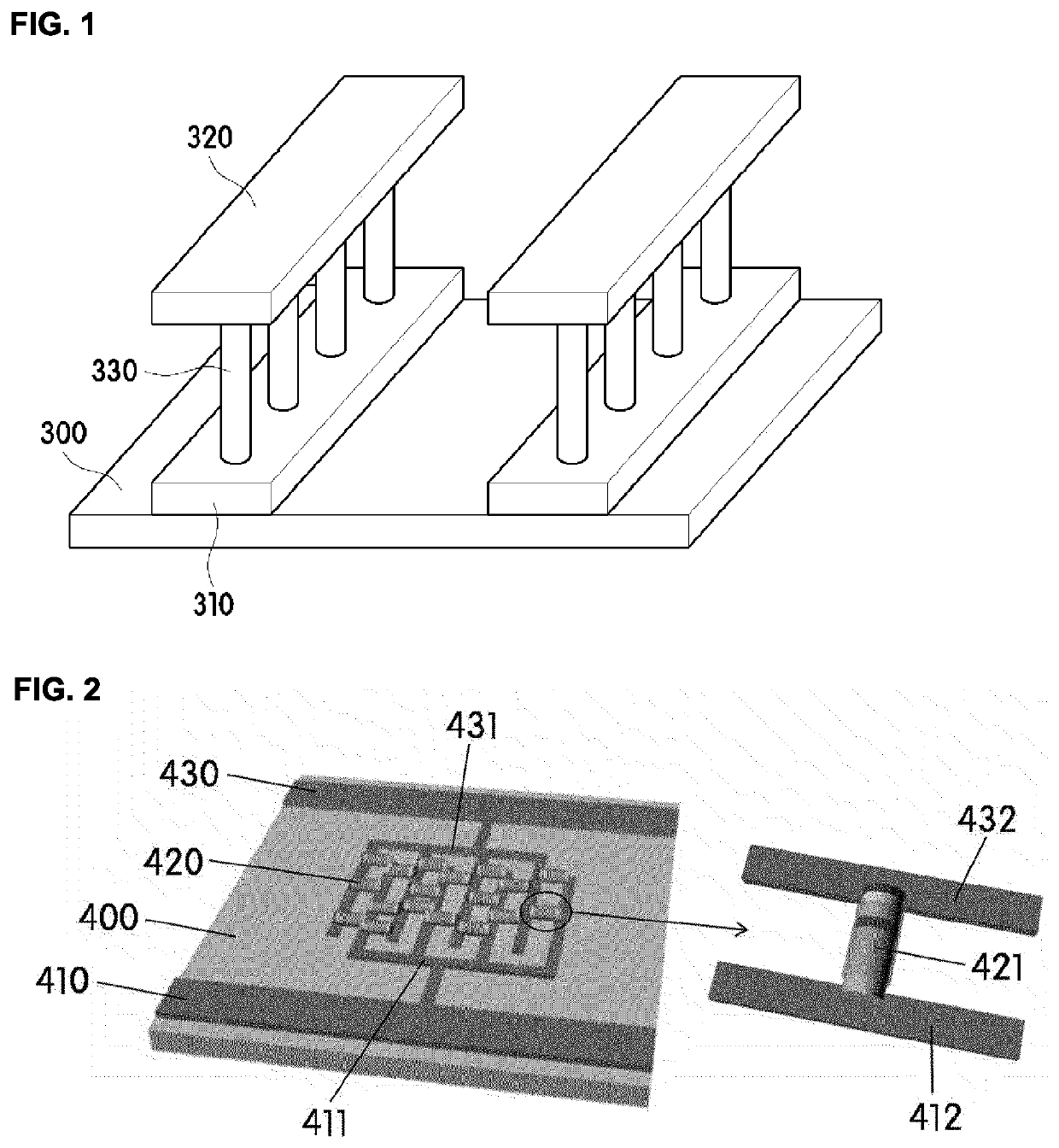
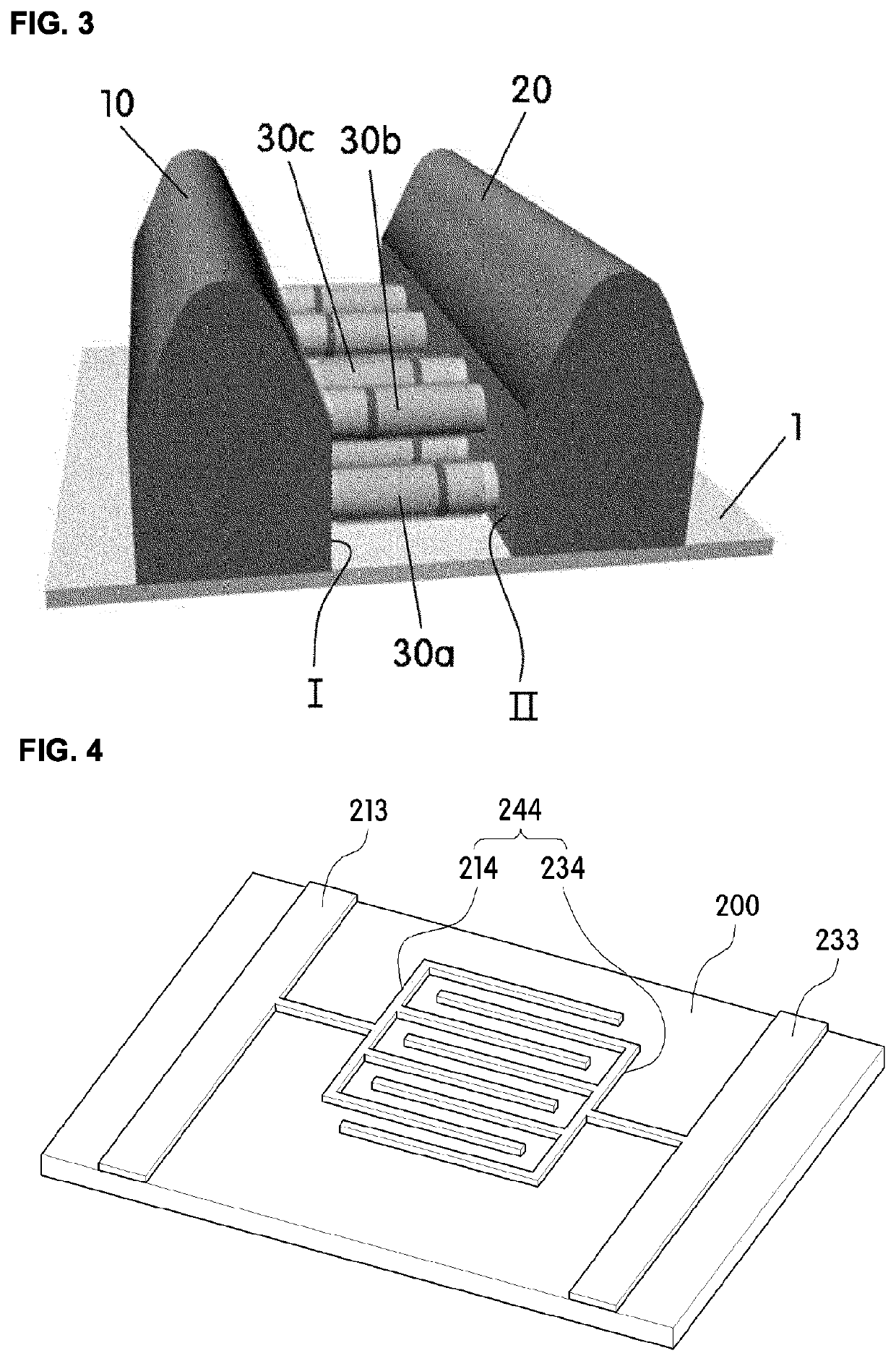
[0052]As is described above, since a nano-scale light emitting diode (LED) element is not disposed and mounted on a target electrode region with a human hand due to a limitation in size of the nano-scale-LED element according to a related art, there is a problem in that it is very difficult for the nano-scale-LED element to be disposed and mounted as intended on an electrode. FIG. 1 is a perspective view of a typical electrode assembly including a nano-scale-LED element, and illustrates a first electrode 310 formed over a base substrate 300, a second electrode 320 formed on the first electrode 310 to be separated therefrom and in parallel therewith, and a nano-scale-LED element 330 connected between the first electrode 310 and the second electrode 320 in a three-dimensionally upright form. In the case of an electrode assembly having such ...


PUM

PropertyMeasurementUnit
lengthaaaaaaaaaa
thicknessaaaaaaaaaa
widthaaaaaaaaaa

Abstract

The present invention relates to an electrode assembly comprising nano-scale-LED elements and a method for manufacturing the same and, more specifically, to an electrode assembly comprising nano-scale-LED elements and a method for manufacturing the same, in which the number of nano-scale-LED elements included in a unit area of the electrode assembly is increased, the light extraction efficiency of individual nano-scale-LED elements is increased so as to maximize light intensity per unit area, and at the same time, nano-scale-LED elements on a nanoscale are connected to an electrode without a fault such as an electrical short circuit.

Description

CROSS-REFERENCE TO RELATED APPLICATIONS[0001]This application is a national phase application under 35 U.S.C. § 371 of International Application No. PCT / KR2015 / 012250, filed Nov. 13, 2015, which claims priority to Korean Patent Application No. 10-2014-0161065, filed Nov. 18, 2014, the contents of which applications are incorporated into the present application by reference.TECHNICAL FIELD[0002]The present disclosure relates to an electrode assembly including nano-scale-light emitting diode (LED) elements and a method for manufacturing the same, and more particularly, to an electrode assembly including nano-scale-LED elements and a method for manufacturing the same, which are capable of maximizing light intensity of the electrode assembly per unit area by increasing the number of nano-scale-LED elements included in a unit area of the electrode assembly and light extraction efficiency of each of the nano-scale-LED elements, and, at the same time, are capable of connecting the nano-sca...

Claims


Application Information

Patent Timeline
Patent Type & Authority Patents(United States)
IPC IPC(8): H01L33/08B82B3/00H01L33/00H01L33/06H01L33/24H01L33/32H01L33/38H01L33/44
CPCH01L33/08B82B3/0066H01L33/007H01L33/06H01L33/24H01L33/32H01L33/387H01L33/44H01L2933/0016H01L25/0753H01L33/36H01L33/38
Inventor SUNG, YEON GOOG
Owner SAMSUNG DISPLAY CO LTD
Learn More