
Input coupler for chip-scale laser receiver device

a laser receiver and input coupler technology, applied in the field of laser receiver devices, can solve the problems of increasing the size and weight of laser receivers, consuming an appreciable amount of power of laser receivers, and complicating the design and operation of platforms, so as to reduce the size, weight and power requirements of platforms, and the effect of reducing the size and weigh

Active Publication Date: 2020-11-24
THE BOEING CO
View PDF48 Cites 1 Cited by
  • Summary
  • Abstract
  • Description
  • Claims
  • Application Information

AI Technical Summary

Benefits of technology

The present patent relates to a laser receiver device that is smaller, lighter, and consumes less power than conventional devices. It includes an input coupler that reduces the loss of light coupling caused by beam jitter, ensuring efficient operation even at reduced power consumption. The use of WDM tunable optical filters and photodetectors further reduces the size, weight, and power requirements. The laser receiver device of the patent can be used in airborne or spaceborne platforms, providing a compact and efficient solution for various applications.

Problems solved by technology

However, mechanical nutators in combination with fiber-optic based WDM components and discrete photodetectors undesirably increase the size and weight of the laser receiver.
Moreover, a laser receiver that includes a mechanical nutator, fiber-optic based WDM components and discrete photodetectors may also consume an appreciable amount of power.
Particularly in instances in which the laser receiver is to be onboard a platform that is to be launched, the size and weight requirements, as well as the power consumption of the laser receiver including the mechanical nutator, the fiber-optic based WDM components and the discrete photodetectors may complicate the design and operation of the platform.

Method used


Image

  • Input coupler for chip-scale laser receiver device
  • Input coupler for chip-scale laser receiver device
  • Input coupler for chip-scale laser receiver device

Examples


Embodiment Construction

[0022]Some embodiments of the present disclosure will now be described more fully hereinafter with reference to the accompanying drawings, in which some, but not all embodiments of the inventions are shown. Indeed, these inventions may be embodied in many different forms and should not be construed as limited to the embodiments set forth herein; rather, these embodiments are provided so that this disclosure will satisfy applicable legal requirements. Like numbers refer to like elements throughout. As used herein, the terms “data,”“content,”“information,” and similar terms may be used interchangeably to refer to data capable of being transmitted, received, and / or stored in accordance with embodiments of the present disclosure. Thus, use of any such terms should not be taken to limit the spirit and scope of embodiments of the present disclosure.

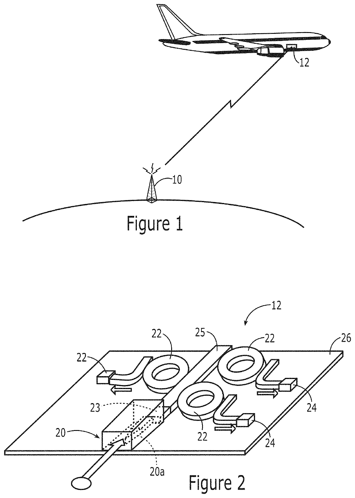
[0023]Laser and other optical communications are conducted between a transmitter and one or more receivers. As shown in FIG. 1, for example, l...


PUM

PropertyMeasurementUnit
lengthaaaaaaaaaa
lengthaaaaaaaaaa
lengthaaaaaaaaaa

Abstract

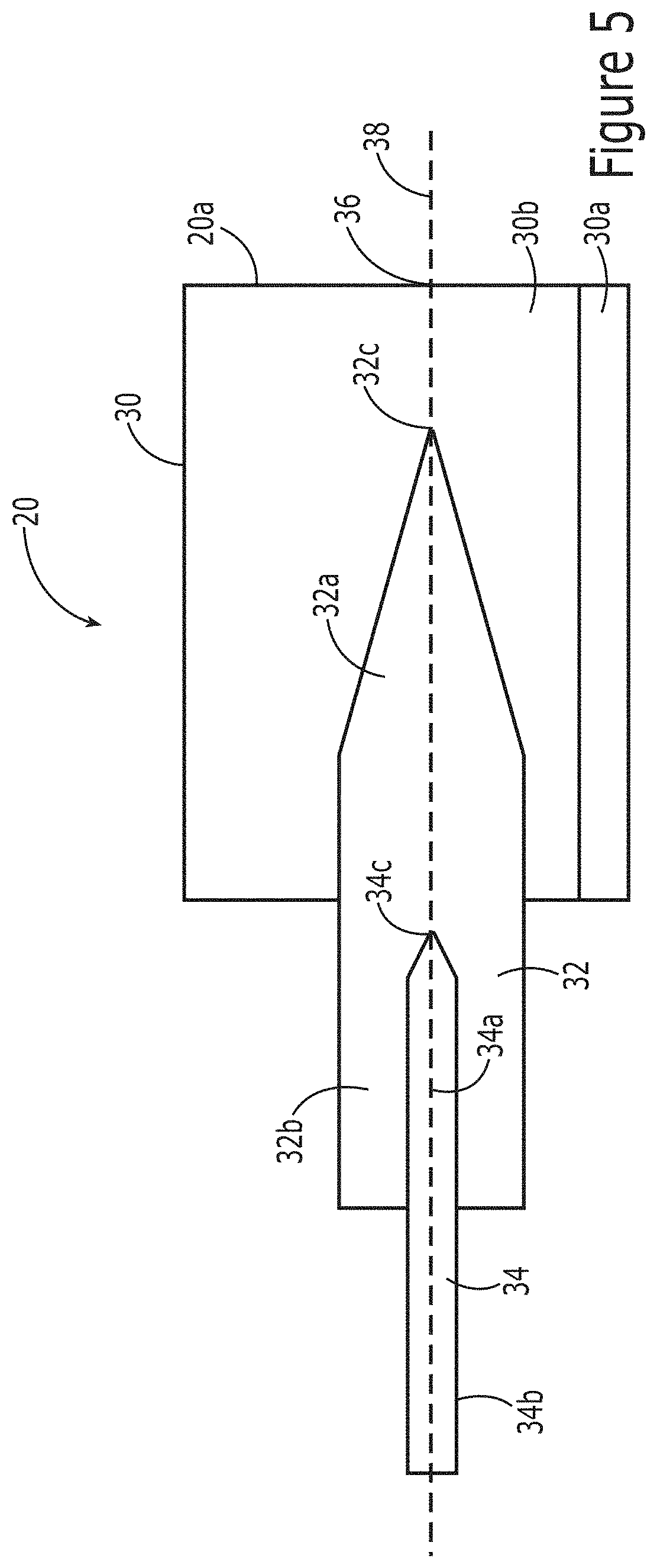
A laser receiver device and an associated input coupler are provided. In this regard, a chip-scale laser receiver device is provided that includes an input coupler that is configured to receive a gaussian beam. The input coupler includes a first waveguide having an optically-transparent material and a second waveguide coupled to the first waveguide. The second waveguide has a tapered configuration that tapers to a predetermined width across a length of not less than 500 micrometers. The input coupler further includes a third waveguide coupled to the second waveguide. The third waveguide has a tapered configuration that tapers to a predetermined width across a length of not less than 250 micrometers. The chip-scale laser receiver device further includes a bus optical waveguide coupled to receive a signal output from the input coupler, and to output a wavelength-multiplexed laser signal.

Description

TECHNOLOGICAL FIELD[0001]An example embodiment relates generally to a laser receiver device and, more particularly, to a chip-scale laser receiver device configured to mitigate the loss of light coupling to a receiver due to beam jitter.BACKGROUND[0002]In communication applications, a signal is transmitted by a transmitter to a receiver, such as from a laser transmitter to a laser receiver in conjunction with laser communications. For efficient and effective communications, the receiver is configured to receive the greatest percentage of the optical signals with the minimum loss.[0003]A laser receiver device may include a mechanical nutator, fiber-optic based wavelength-division-multiplexed (WDM) components and discrete photodetectors. The mechanical nutator receives the laser communication signals and transmits those signals to the fiber-optic based WDM components. The laser communication signals generally include signals at each of a plurality of different wavelengths. Thus, the f...

Claims


Application Information

Patent Timeline
Patent Type & Authority Patents(United States)
IPC IPC(8): G02B6/42H04B10/25H04B10/50H04B10/67H04J14/02G02B6/293
CPCH04J14/02H04B10/503G02B6/2938G02B6/4215G02B6/29343H04B10/67G02B6/29395G02B6/42H04B10/25891G02B6/4206G02B6/12007G02B6/1228G02B6/29347H04B10/1121
Inventor EFIMOV, OLEG M.HUANG, BIQINPATTERSON, PAMELA R.SARKISSIAN, RAYMONDSAYYAH, KEYVAN
Owner THE BOEING CO
Learn More